ZHCSLB8C May 2020 – May 2021 LMH9235
PRODUCTION DATA
- 1 特性
- 2 應(yīng)用
- 3 說明
- 4 Revision History
- 5 Pin Configuration and Functions
- 6 Specifications
- 7 Detailed Description
- 8 Application and Implementation
- 9 Power Supply Recommendations
- 10Layout
- 11Device and Documentation Support
- 12Mechanical, Packaging, and Orderable Information
封裝選項
機械數(shù)據(jù) (封裝 | 引腳)
- RRL|12
散熱焊盤機械數(shù)據(jù) (封裝 | 引腳)
訂購信息
5 Pin Configuration and Functions
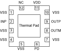
 Figure 5-1 RRL Package12-Pin WQFNTop View
Table 5-1 Pin Functions
| PIN | I/O | DESCRIPTION | |
|---|---|---|---|
| NO. | NAME | ||
| 1 | VSS | Power | Ground |
| 2 | INP | Input | RF single-ended input into amplifier |
| 3 | VSS | Power | Ground |
| 4 | VSS | Power | Ground |
| 5 | VSS | Power | Ground |
| 6 | PD | Input | Power down connection. PD = 0 V = normal operation; PD = 1.8 V = power off mode. |
| 7 | VSS | Power | Ground |
| 8 | OUTM | Output | RF differential output negative |
| 9 | OUTP | Output | RF differential output positive |
| 10 | VSS | Power | Ground |
| 11 | VDD | Power | Positive supply voltage (3.3 V) |
| 12 | NC | — | Do not connect this pin |
| Thermal Pad | — | Connect the thermal pad to Ground | |