SDAA192 November 2025 UCC33020 , UCC33020-Q1 , UCC33410 , UCC33410-Q1 , UCC33420 , UCC33420-Q1
2.3 PCB Layout
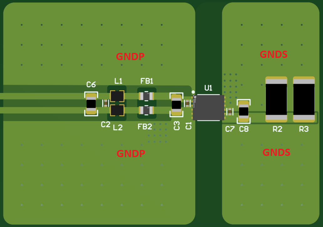
The placement of ground planes on both primary and secondary side provides low impedance at the return of the switching loop when used to connect the ground pins of the device. What is more, these planes act as Faraday shields, mitigating the H field coming from the transformer. Apply the largest copper area that the design allows.
 Figure 2-15 Ground Planes in PCB
To prevent any bypass of the HF currents through the layout parasitic capacitance, it is recommended removing copper underneath the DM inductors and FBs. For the same reason, we recommend a 1mm KOZ around the EMI filter area.
 Figure 2-16 KOZ and Copper Cut Under DM Inductors
and FB
Figure 2-16 KOZ and Copper Cut Under DM Inductors
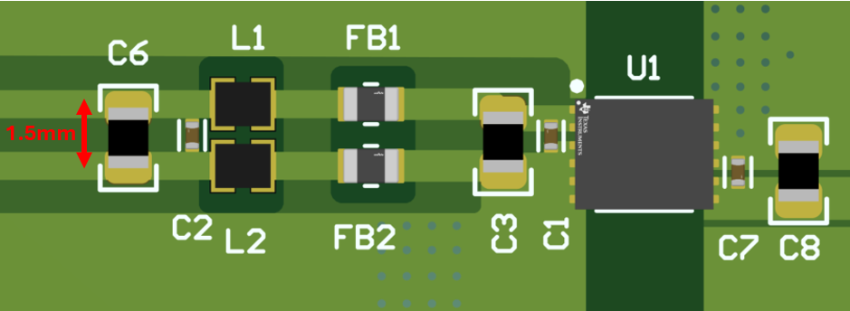
and FBDue to the impedance match on both sides of the switching loop (positive and return), the CM noise is minimized, and the switching loop distance does not affect the EMI at the LISN. Because of this, it is recommended to keep the switching loop as short to keep a low footprint design. In this case, a 1.5mm distance for the switching loop is selected.
 Figure 2-17 Switching Loop Distance