ZHCS779C March 2012 – July 2025 UCC28070 , UCC28070A
PRODUCTION DATA
- 1
- 1 特性
- 2 應(yīng)用
- 3 說(shuō)明
- 4 Pin Configuration and Functions
- 5 Specifications
-
6 Detailed Description
- 6.1 Overview
- 6.2 Functional Block Diagram
- 6.3
Feature Description
- 6.3.1 Interleaving
- 6.3.2 Programming the PWM Frequency and Maximum Duty-Cycle Clamp
- 6.3.3 Frequency Dithering (Magnitude and Rate)
- 6.3.4 External Clock Synchronization
- 6.3.5 Multi-phase Operation
- 6.3.6 VSENSE and VINAC Resistor Configuration
- 6.3.7 VSENSE and VINAC Open-Circuit Protection
- 6.3.8 Current Synthesizer
- 6.3.9 Programmable Peak Current Limit
- 6.3.10 Linear Multiplier and Quantized Voltage Feed Forward
- 6.3.11 Enhanced Transient Response (VA Slew-Rate Correction)
- 6.3.12 Bias Voltages (VCC and VREF)
- 6.3.13 PFC Enable and Disable
- 6.3.14 Adaptive Soft-Start
- 6.3.15 PFC Start-Up Hold Off
- 6.3.16 Output Overvoltage Protection (OVP)
- 6.3.17 Zero-Power Detection
- 6.3.18 Thermal Shutdown
- 6.3.19 Current Loop Compensation
- 6.3.20 Voltage Loop Compensation
- 6.4 Device Functional Modes
-
7 Application and Implementation
- 7.1 Application Information
- 7.2
Typical Application
- 7.2.1 Design Requirements
- 7.2.2
Detailed Design Procedure
- 7.2.2.1 Output Current Calculation
- 7.2.2.2 Bridge Rectifier
- 7.2.2.3 PFC Inductor (L1 and L2)
- 7.2.2.4 PFC MOSFETs (M1 and M2)
- 7.2.2.5 PFC Diode
- 7.2.2.6 PFC Output Capacitor
- 7.2.2.7 Current-Loop Feedback Configuration (Sizing of the Current-Transformer Turns-Ratio NCT and Current-Sense Resistor RS)
- 7.2.2.8 Current-Sense Offset and PWM Ramp for Improved Noise Immunity
- 7.2.3 Application Curves
- 7.3 Power Supply Recommendations
- 7.4 Layout
- 8 器件和文檔支持
- 9 Revision History
- 10Mechanical, Packaging, and Orderable Information
封裝選項(xiàng)
機(jī)械數(shù)據(jù) (封裝 | 引腳)
- PW|20
散熱焊盤機(jī)械數(shù)據(jù) (封裝 | 引腳)
訂購(gòu)信息
7.2.2.8 Current-Sense Offset and PWM Ramp for Improved Noise Immunity
To improve noise immunity at extremely light loads, TI recommends adding a PWM ramp with a DC offset to the current-sense signals. Electrical components RTA, RTB, ROA, ROB, CTA, CTB, DPA1, DPA2, DPB1, DPB1 CTA, and CTB form a PWM ramp that is activated and deactivated by the gate drive outputs of the UCC28070A. Resistor ROA and ROB add a DC offset to the CS resistors (RSA and RSB).
 Figure 7-4 PWM Ramp and Offset Circuit
When the inductor current becomes discontinuous the boost inductors ring with the parasitic capacitances in the boost stages. This inductor current rings through the CTs causing a false current-sense signal. Figure 7-5 shows what the current-sense signal looks like when the inductor current becomes discontinuous.
The inductor current (IL1) and VRsa may vary from this graphical representation depending on how much inductor ringing is in the design when the current becomes discontinuous.
 Figure 7-5 False Current-Sense
Signal
Figure 7-5 False Current-Sense
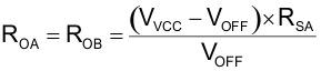
SignalTo counter for the offset (VOFF) just requires adjusting resistors ROA and ROB to ensure that when the unit goes discontinuous the current-sense resistor is not seeing a positive current when it must be zero. Setting the offset to 100mV is a good initial starting point and can be adjusted down or up based on evaluation of THDi.

A small ramp with ΔV that is equal to [10% of the maximum current-sense signal (VS) minus the offset] can also be added by selecting RTA, RTB, CTA and CTB as follows.