ZHCSP68C December 2021 – October 2022 DRV8328
PRODUCTION DATA
- 1 特性
- 2 應(yīng)用
- 3 說明
- 4 Revision History
- 5 Device Comparison Table
- 6 Pin Configuration and Functions
- 7 Specification
-
8 Detailed Description
- 8.1 Overview
- 8.2 Functional Block Diagram
- 8.3
Feature Description
- 8.3.1 Three BLDC Gate Drivers
- 8.3.2 AVDD Linear Voltage Regulator
- 8.3.3 Pin Diagrams
- 8.3.4 Gate Driver Shutdown Sequence (DRVOFF)
- 8.3.5
Gate Driver Protective Circuits
- 8.3.5.1 PVDD Supply Undervoltage Lockout (PVDD_UV)
- 8.3.5.2 AVDD Power on Reset (AVDD_POR)
- 8.3.5.3 GVDD Undervoltage Lockout (GVDD_UV)
- 8.3.5.4 BST Undervoltage Lockout (BST_UV)
- 8.3.5.5 MOSFET VDS Overcurrent Protection (VDS_OCP)
- 8.3.5.6 VSENSE Overcurrent Protection (SEN_OCP)
- 8.3.5.7 Thermal Shutdown (OTSD)
- 8.4 Device Functional Modes
-
9 Application and Implementation
- 9.1 Application Information
- 9.2
Typical Application
- 9.2.1
Three Phase Brushless-DC Motor Control
- 9.2.1.1
Detailed Design Procedure
- 9.2.1.1.1 Motor Voltage
- 9.2.1.1.2 Bootstrap Capacitor and GVDD Capacitor Selection
- 9.2.1.1.3 Gate Drive Current
- 9.2.1.1.4 Gate Resistor Selection
- 9.2.1.1.5 System Considerations in High Power Designs
- 9.2.1.1.6 Dead Time Resistor Selection
- 9.2.1.1.7 VDSLVL Selection
- 9.2.1.1.8 AVDD Power Losses
- 9.2.1.1.9 Power Dissipation and Junction Temperature Losses
- 9.2.1.1
Detailed Design Procedure
- 9.2.2 Application Curves
- 9.2.1
Three Phase Brushless-DC Motor Control
- 10Power Supply Recommendations
- 11Layout
- 12Device and Documentation Support
- 13Mechanical, Packaging, and Orderable Information
封裝選項(xiàng)
機(jī)械數(shù)據(jù) (封裝 | 引腳)
- RUY|28
散熱焊盤機(jī)械數(shù)據(jù) (封裝 | 引腳)
訂購(gòu)信息
9.2.2 Application Curves
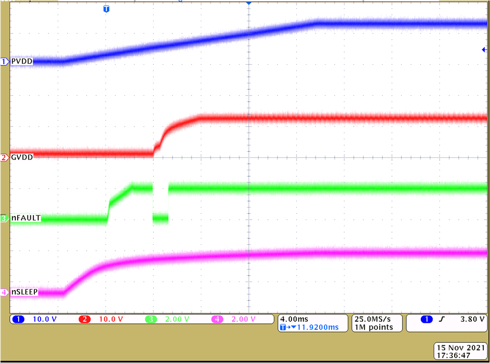 Figure 9-8 Device Powerup with PVDD
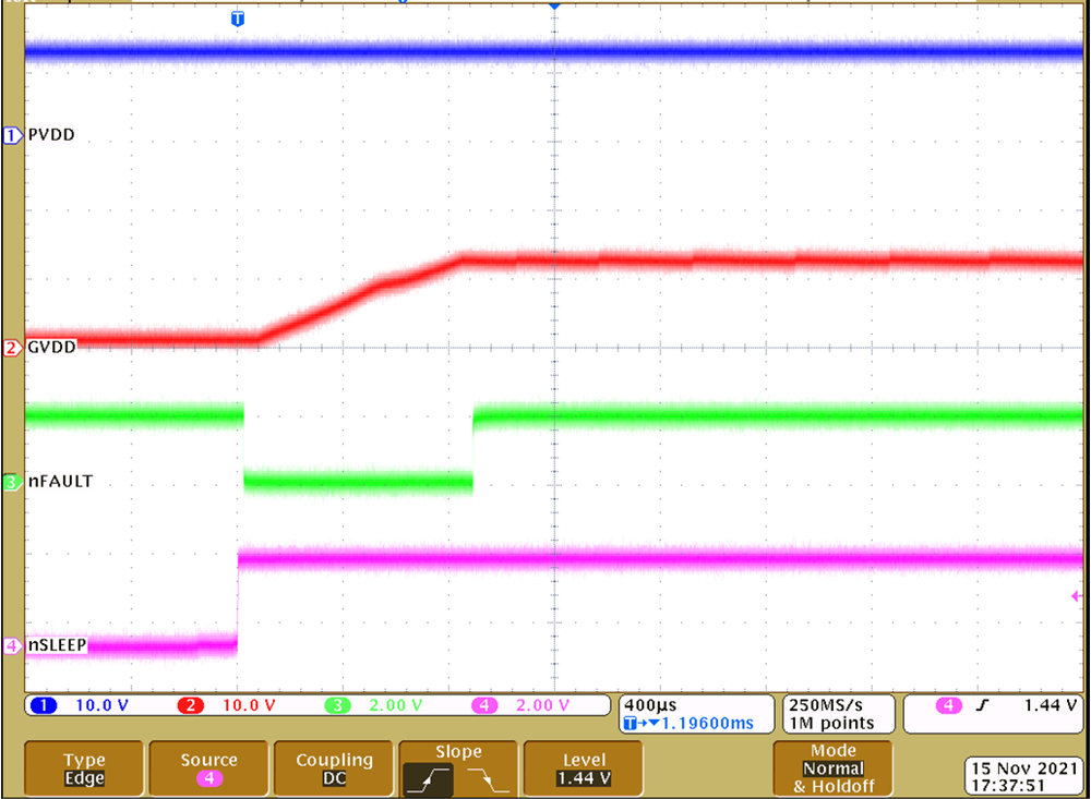 Figure 9-9 Device Powerup with nSLEEP
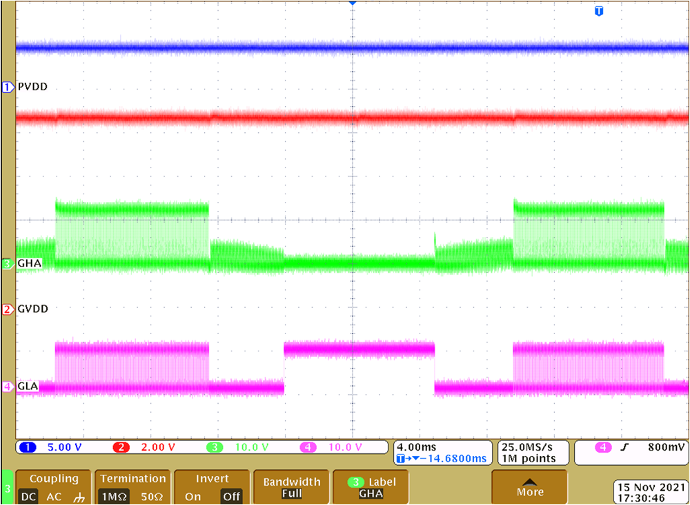 Figure 9-10 GVDD voltage threshold (PVDD = 4.5 V)
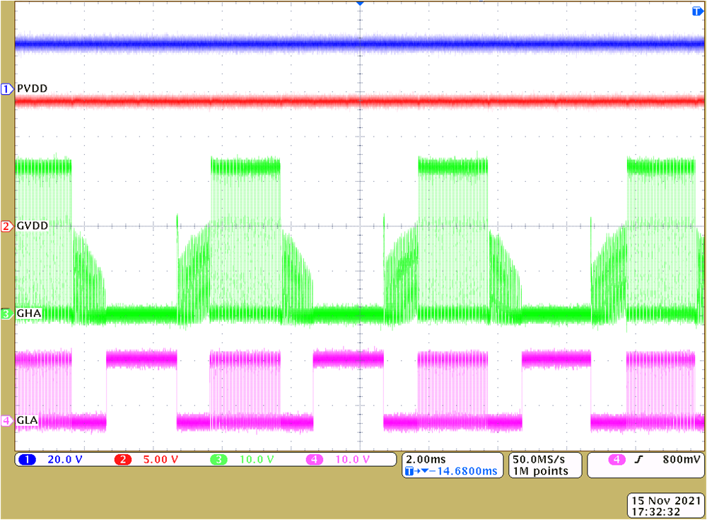 Figure 9-11 GVDD voltage threshold (PVDD = 20V)
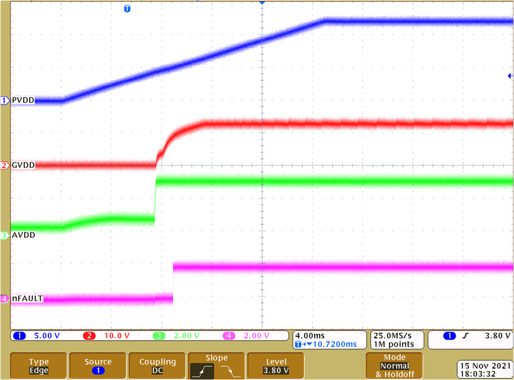 Figure 9-12 AVDD powerup
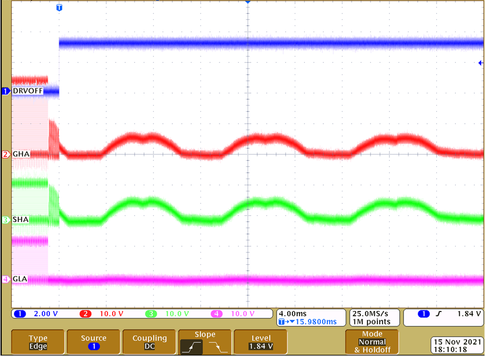 Figure 9-13 DRVOFF operation
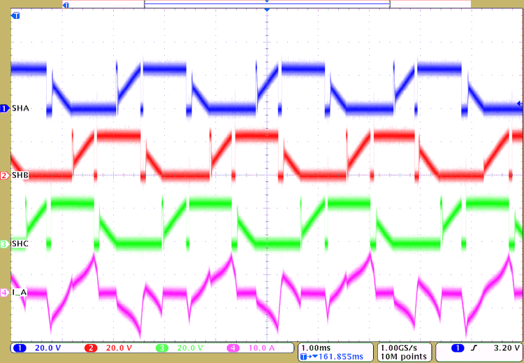 Figure 9-14 Driver operation at 100% duty cycle
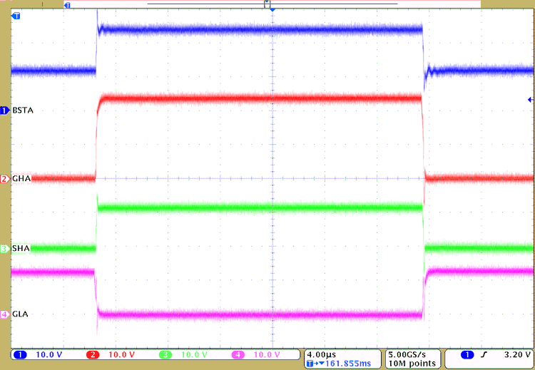 Figure 9-15 Driver PWM operation, 20 kHz, 50% duty cycle, zoomed
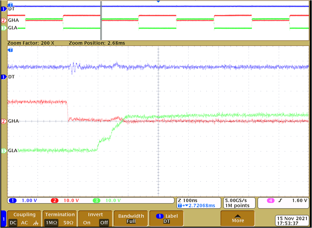 Figure 9-16 Driver dead time of 100 ns (DT = 10 kΩ to GND)
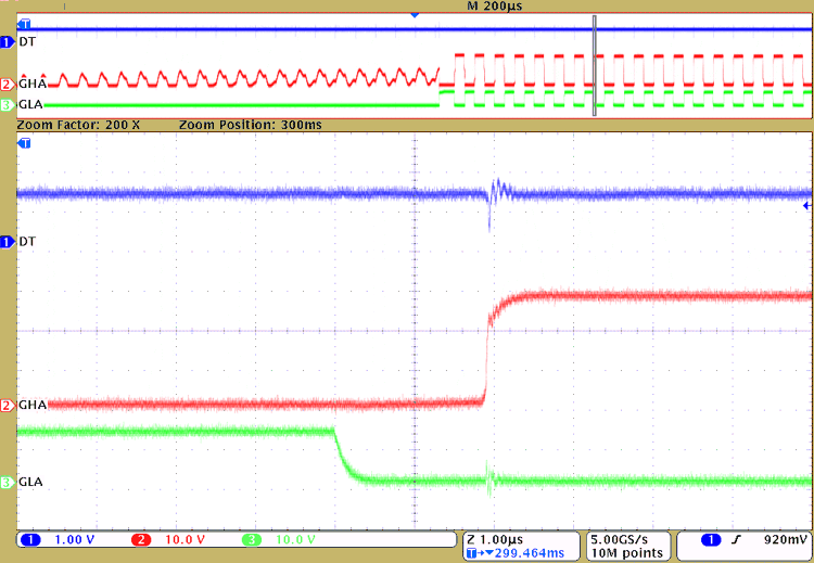 Figure 9-17 Driver dead time of 2000 ns (DT = 390 kΩ to GND)
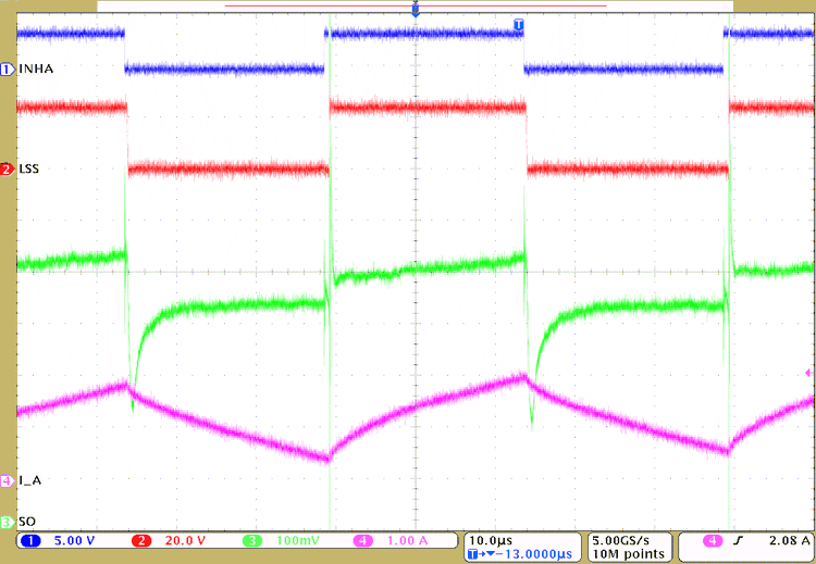 Figure 9-18 Current sense amplifier operation (GAIN = 40 V/V)