ZHCSMX2C June 2007 – December 2024 TRS3221E
PRODUCTION DATA
- 1
- 1 特性
- 2 應(yīng)用
- 3 說(shuō)明
- 4 Pin Configuration and Functions
-
5 Specifications
- 5.1 Absolute Maximum Ratings
- 5.2 ESD Ratings
- 5.3 ESD Ratings, IEC Specifications
- 5.4 Recommended Operating Conditions
- 5.5 Thermal Information
- 5.6 Electrical Characteristics
- 5.7 Driver Section Electrical Characteristics
- 5.8 Driver Section Switching Characteristics
- 5.9 Receiver Section Electrical Characteristics
- 5.10 Receiver Section Switching Characteristics
- 5.11 Auto-Powerdown Section Electrical Characteristics
- 5.12 Auto-Powerdown Section Switching Characteristics
- 5.13 Typical Characteristics
- 6 Parameter Measurement Information
- 7 Detailed Description
- 8 Application Information Disclaimer
- 9 Device and Documentation Support
- 10Revision History
- 11Mechanical, Packaging, and Orderable Information
封裝選項(xiàng)
機(jī)械數(shù)據(jù) (封裝 | 引腳)
散熱焊盤(pán)機(jī)械數(shù)據(jù) (封裝 | 引腳)
- RGT|16
訂購(gòu)信息
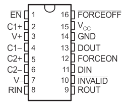
4 Pin Configuration and Functions
 Figure 4-1 16-Pin SSOP (DB) or TSSOP (PW)
Packages, Top View
 Figure 4-2 16-pin VQFN (RGT) Package, Top
View
Figure 4-2 16-pin VQFN (RGT) Package, Top
ViewTable 4-1 Pin Functions
| PIN | TYPE | DESCRIPTION | ||
|---|---|---|---|---|
| NAME | DB or PW | RGT | ||
| C1+ | 2 | 16 | — | Positive terminals of the voltage-doubler charge-pump capacitors |
| C2+ | 5 | 2 | — | |
| C1– | 4 | 1 | — | Negative terminals of the voltage-doubler charge-pump capacitors |
| C2– | 6 | 3 | — | |
| DIN | 11 | 8 | I | Driver input |
| DOUT | 13 | 10 | O | RS-232 driver output |
| EN | 1 | 14 | I | Low input enables receiver ROUT output. High input sets ROUT to high impedance. |
| FORCEOFF | 16 | 13 | I | Automatic power-down control input |
| FORCEON | 12 | 9 | I | Automatic power-down control input |
| GND | 14 | 11 | GND | Ground |
| INVALID | 10 | 7 | O | Invalid output pin. Output is low when all RIN inputs are unpowered. |
| RIN | 8 | 5 | I | RS-232 receiver input |
| ROUT | 9 | 6 | O | Receiver output |
| VCC | 15 | 12 | — | 3V to 5.5V supply voltage |
| V+ | 3 | 15 | O | 5.5V supply generated by the charge pump |
| V– | 7 | 4 | O | –5.5V supply generated by the charge pump |
| Thermal Pad | None | Thermal Pad | - | Exposed thermal pad. Can be connected to GND or left floating. |
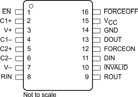
 Figure 4-3 DYY Package
16-Pin SOT-23-THN
(Top View)
Table 4-2 Pin Functions
| PIN | TYPE | DESCRIPTION | |
|---|---|---|---|
| NAME | NO. | ||
| C1+ | 2 | — | Positive terminals of the voltage-doubler charge pump capacitors |
| C2+ | 5 | ||
| C1– | 4 | — | Negative terminals of the voltage-doubler charge pump capacitors |
| C2– | 6 | ||
| DIN | 11 | I | Driver input |
| DOUT | 13 | O | RS-232 driver output |
| EN | 1 | I | Low input enables receiver ROUT output. High input sets ROUT to high impedance. |
| FORCEOFF | 16 | I | Automatic power-down control input |
| FORCEON | 12 | I | Automatic power-down control input |
| GND | 14 | — | Ground |
| INVALID | 10 | O | Invalid output pin. Output low when RIN input is unpowered. |
| RIN | 8 | I | RS-232 receiver input |
| ROUT | 9 | O | Receiver output |
| VCC | 15 | — | 3V to 5.5V supply voltage |
| V+ | 3 | O | 5.5V supply generated by the charge pump |
| V– | 7 | O | –5.5V supply generated by the charge pump |