ZHCSI58C October 2009 – May 2018 TPS65720 , TPS65721
PRODUCTION DATA.
- 1 特性
- 2 應(yīng)用
- 3 說(shuō)明
- 4 修訂歷史記錄
- 5 Device Options
- 6 Pin Configuration and Functions
- 7 Specifications
-
8 Detailed Description
- 8.1 Overview
- 8.2 Functional Block Diagrams
- 8.3
Feature Description
- 8.3.1 Battery Charger and Power Path
- 8.3.2 Power-Path Management
- 8.3.3 Battery Charging
- 8.3.4 Thermal Regulation and Thermal Shutdown
- 8.3.5 Battery Pack Temperature Monitoring
- 8.3.6 DCDC1 Converter
- 8.3.7 Power Save Mode
- 8.3.8 Short-Circuit Protection
- 8.3.9 Thermal Shutdown
- 8.3.10 LDO1
- 8.4 Device Functional Modes
- 8.5 Programming
- 8.6
Register Maps
- 8.6.1 CHGSTATUS Register Address: 01h (read only)
- 8.6.2 CHGCONFIG0 Register Address: 02h (read/write)
- 8.6.3 CHGCONFIG1 Register Address: 03h (read/write)
- 8.6.4 CHGCONFIG2 Register Address: 04h (read/write)
- 8.6.5 CHGCONFIG3 Register Address: 05h (read/write)
- 8.6.6 CHGSTATE Register Address: 06h (read only)
- 8.6.7 DEFDCDC1 Register Address: 07h (read/write)
- 8.6.8 LDO_CTRL Register Address: 08h (read/write)
- 8.6.9 CONTROL0 Register Address: 09h (read/write)
- 8.6.10 CONTROL1 Register Address: 0Ah (read/write)
- 8.6.11 GPIO_SSC Register Address: 0Bh (read/write)
- 8.6.12 GPIODIR Register Address: 0Ch (read/write)
- 8.6.13 IRMASK0 Register Address: 0Dh (read/write)
- 8.6.14 IRMASK1 Register Address: 0Eh (read/write)
- 8.6.15 IRMASK2 Register Address: 0Fh (read/write)
- 8.6.16 IR0 Register Address: 10h (read only)
- 8.6.17 IR1 Register Address: 11h (read)
- 8.6.18 IR2 Register Address: 12h (read)
- 9 Application and Implementation
- 10Power Supply Recommendations
- 11Layout
- 12器件和文檔支持
- 13機(jī)械、封裝和可訂購(gòu)信息
封裝選項(xiàng)
機(jī)械數(shù)據(jù) (封裝 | 引腳)
- YFF|25
散熱焊盤(pán)機(jī)械數(shù)據(jù) (封裝 | 引腳)
訂購(gòu)信息
9.2.3 Application Curves
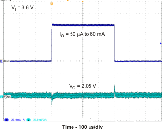
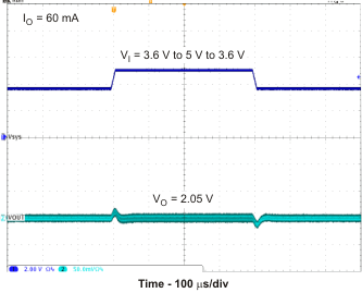
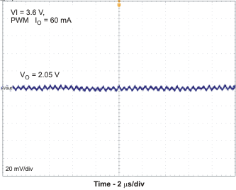
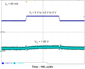
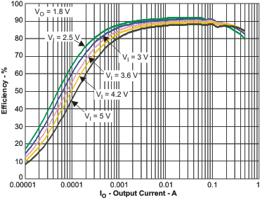
The graphs have been generated on the TPS65720YFF EVM with the inductors as mentioned in the graphs. See the TPS65720EVM User's Guide for details on the layout.
Table 8. Table Of Graphs
| FIGURE | |||
|---|---|---|---|
| TPS65720: Efficiency DCDC1 vs Load Current / PWM mode 200 mA;
L = Murata LQM21P 3.3 μH |
VO = 2.05 V; Vi = 3 V, 3.6 V, 4.2 V, 5 V | Figure 24 | |
| TPS65720: Efficiency DCDC1 vs Load Current / PFM mode 200 mA;
L = Murata LQM21P 3.3 μH |
VO = 2.05 V; Vi = 3 V, 3.6 V, 4.2 V, 5 V | Figure 25 | |
| TPS65720: Efficiency DCDC1 vs Load Current / PWM mode 200 mA;
L = FDK MIPSA2520 2.2 μH |
VO = 2.05 V; VI = 3 V, 3.6 V, 4.2 V, 5 V | Figure 26 | |
| TPS65720: Efficiency DCDC1 vs Load Current / PFM mode 200 mA;
L = FDK MIPSA2520 2.2 μH |
VO = 2.05 V; VI = 3 V, 3.6 V, 4.2 V, 5 V | Figure 27 | |
| TPS65721: Efficiency DCDC1 vs Load Current / PWM mode;
L = FDK MIPSA2520 2.2 μH |
VO = 3.3 V; VI = 3 V, 3.6 V, 4.2 V, 5 V | Figure 28 | |
| TPS65721: Efficiency DCDC1 vs Load Current / PFM mode 500 mA;
L = FDK MIPSA2520 2.2 μH |
VO = 3.3 V; VI = 3 V, 3.6 V, 4.2 V, 5 V | Figure 29 | |
| TPS65721: Efficiency DCDC1 vs Load Current / PWM mode;
L = FDK MIPSA2520 2.2 μH |
VO = 1.8 V; VI = 3 V, 3.6 V, 4.2 V, 5 V | Figure 30 | |
| TPS65721: Efficiency DCDC1 vs Load Current / PFM mode 500 mA;
L = FDK MIPSA2520 2.2 μH |
VO = 1.8 V; VI = 3 V, 3.6 V, 4.2 V, 5 V | Figure 31 | |
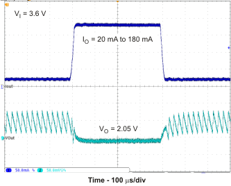
| Load Transient Response DCDC1;
L = FDK MIPSA2520 2.2 μH, PFM mode |
Scope plot
IO = 20 mA to 180 mA; VO = 2.05 V; VI = 3.6 V |
Figure 32 | |
| Load Transient Response DCDC1;
L = FDK MIPSA2520 2.2 μH, PWM mode |
Scope plot
IO = 50 μA to 60 mA; VO = 2.05 V; VI = 3.6 V |
Figure 33 | |
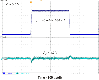
| Load Transient Response DCDC1;
L = FDK MIPSA2520 2.2 μH, PWM mode |
Scope plot
IO = 40 mA to 360 mA; VO = 3.3 V; VI = 3.6 V |
Figure 34 | |
| Line Transient Response DCDC1;
L = FDK MIPSA2520 2.2 μH, PWM mode |
Scope plot; VO = 2.05 V
VI = 3.6 V to 5 V to 3.6 V; IO = 60 mA |
Figure 35 | |
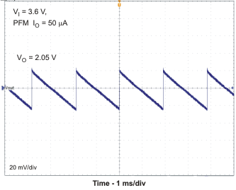
| Output Voltage Ripple in PFM Mode; DCDC1 | Scope plot: VI = 3.6 V
VO = 2.05 V; IO = 50 μA (PFM); IO = 60 mA (PWM) |
Figure 36 | |
| Output Voltage Ripple in PWM Mode; DCDC1 | Scope plot: VI = 3.6 V
VO = 2.05 V; IO = 60 mA (PWM) |
Figure 37 | |
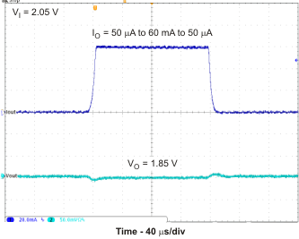
| Load Transient Response LDO1 | Scope plot; V = 1.85 V; VI = 2.05 V
I = 50 μA to 60 mA to 50 μA |
Figure 38 | |
| Line Transient Response LDO1 | Scope plot; VO = 1.85 V; VI = 5 V to 3.6 V to 5 V | Figure 39 | |
| Efficiency vs Lout for DCDC1 = 2.05 V, LDO1 = 1.85 V,
VinLDO = VDCDC1 |
Figure 40 | ||
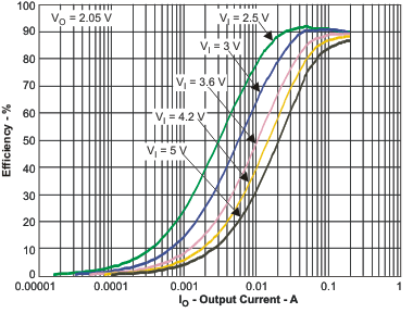
| PWM Mode | Inductor: LQM21P 3.3 µH |
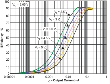
| PWM Mode | Inductor: MIPSA2520 2.2 µH |
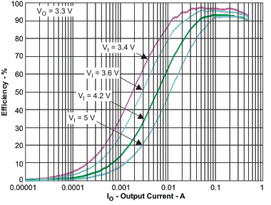
| PWM Mode | Inductor: MIPSA2520 2.2 µH |
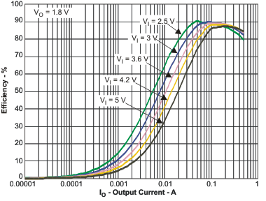
| PWM Mode | Inductor: MIPSA2520 2.2 µH |
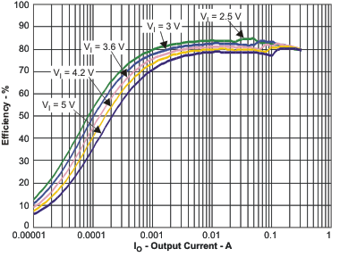
| LDO1 powered by DCDC1
with VDCDC1 = 2.05 V |
VLDO1 = 1.85 V | ||||||
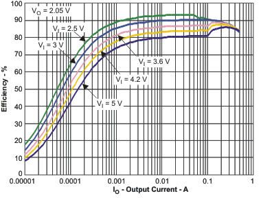
| PFM Mode | Inductor: LQM21P 3.3 µH |
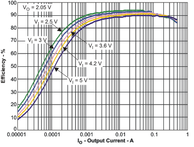
| PFM Mode | Inductor: MIPSA2520 2.2 µH |
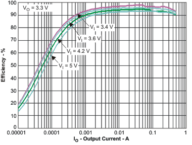
| PFM Mode | Inductor: MIPSA2520 2.2 µH |
| PFM Mode | Inductor: MIPSA2520 2.2 µH |
