ZHCS844D November 2011 – January 2025 TLV70012-Q1 , TLV70018-Q1
PRODUCTION DATA
- 1
- 1 特性
- 2 應用
- 3 說明
- 4 Pin Configuration and Functions
- 5 Specifications
- 6 Detailed Description
- 7 Application and Implementation
- 8 Device and Documentation Support
- 9 Revision History
- 10Mechanical, Packaging, and Orderable Information
封裝選項
機械數(shù)據(jù) (封裝 | 引腳)
- DDC|5
散熱焊盤機械數(shù)據(jù) (封裝 | 引腳)
訂購信息
4 Pin Configuration and Functions
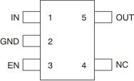
 Figure 4-1 DDC Package,5-Pin SOT(Top View)
Table 4-1 Pin Functions
| PIN | DESCRIPTION | |
|---|---|---|
| NO. | NAME | |
| 1 | IN | Input pin. A small 1μF ceramic capacitor is recommended from this pin to ground to provide stability and good transient performance.(1) |
| 2 | GND | Ground pin |
| 3 | EN | Enable pin. Driving EN over 0.9V turns on the regulator. Driving EN below 0.4V puts the regulator into shutdown mode and reduces operating current to 1μA, nominal. |
| 4 | NC | No connection. This pin can be tied to ground to improve thermal dissipation. |
| 5 | OUT | Regulated output voltage pin. A small 1μF ceramic capacitor is needed from this pin to ground to provide stability.(1) |
(1) See the Input and Output Capacitor Requirements section for more details.