SLOS454I January 2005 – July 2016 THS4509
PRODUCTION DATA.
- 1 Features
- 2 Applications
- 3 Description
- 4 Revision History
- 5 Device Comparison Table
- 6 Pin Configuration and Functions
- 7 Specifications
- 8 Detailed Description
- 9 Application and Implementation
- 10Power Supply Recommendations
- 11Layout
- 12Device and Documentation Support
- 13Mechanical, Packaging, and Orderable Information
封裝選項
機械數(shù)據(jù) (封裝 | 引腳)
- RGT|16
散熱焊盤機械數(shù)據(jù) (封裝 | 引腳)
- RGT|16
訂購信息
11 Layout
11.1 Layout Guidelines
It is recommended to follow the layout of the external components near the amplifier, ground plane construction, and power routing of the EVM as closely as possible.
11.1.1 General Guidelines
- Signal routing should be direct and as short as possible into and out of the op amp circuit.
- The feedback path should be short and direct; avoid vias.
- Ground or power planes should be removed from directly under the amplifier input and output pins.
- An output resistor is recommended on each output, as near to the output pin as possible.
- Two 10-μF and two 0.1-μF power-supply decoupling capacitors must be placed as near to the power-supply pins as possible.
- Two 0.1-μF capacitors must be placed between the CM input pins and ground. This configuration limits noise coupled into the pins. One each must be placed to ground near pin 4 and pin 9.
- TI recommends splitting the ground panel on layer 2 (L2) as shown below and to use a solid ground on layer 3 (L3). A single-point connection must be used between each split section on L2 and L3.
- A single-point connection to ground on L2 is recommended for the input termination resistors R1 and R2. This configuration must be applied to the input gain resistors if termination is not used.
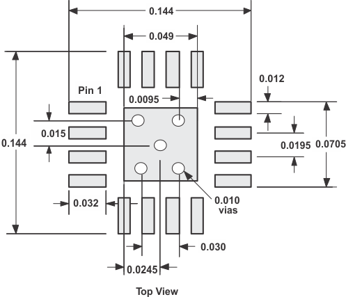
- The THS4509 recommended PCB footprint is shown in Figure 92.
11.1.2 PowerPAD PCB Layout Considerations
Although there are many ways to properly heatsink the PowerPAD package, the following steps illustrate the recommended approach:
- Prepare the PCB with a top side etch pattern as shown in Figure 92. There must be etch for the leads as well as etch for the thermal pad.
- Place five holes in the area of the thermal pad. The holes must be 13 mils (0.013 in, 0.33 mm) in diameter. Keep them small so that solder wicking through the holes is not a problem during reflow.
- Additional vias may be placed anywhere along the thermal plane outside of the thermal pad area. They help dissipate the heat generated by the IC. These additional vias may be larger than the 13-mil diameter vias directly under the thermal pad. They can be larger because they are not in the thermal pad area to be soldered, so that wicking is not a problem.
- Connect all holes to the internal ground plane.
- When connecting these holes to the ground plane, do not use the typical web or spoke via connection methodology. Web connections have a high thermal resistance connection that is useful for slowing the heat transfer during soldering operations. This resistance makes the soldering of vias that have plane connections easier. In this application, however, low thermal resistance is desired for the most efficient heat transfer. Therefore, the holes under the IC PowerPAD package should make the connection to the internal ground plane, with a complete connection around the entire circumference of the plated-through hole.
- The top-side solder mask must leave the terminals of the package and the thermal pad area with its five holes exposed. The bottom-side solder mask should cover the five holes of the thermal pad area. This configuration prevents solder from being pulled away from the thermal pad area during the reflow process.
- Apply solder paste to the exposed thermal pad area and all of the IC terminals.
- With these preparatory steps in place, the IC is simply placed in position and run through the solder reflow operation as any standard surface-mount component. This process results in a part that is properly installed.
 Figure 92. PowerPAD PCB Etch and Via Pattern
The next consideration is the package constraints. The two sources of heat within an amplifier are quiescent power and output power. The designer must never forget about the quiescent heat generated within the device, especially multi-amplifier devices. Because these devices have linear output stages (Class AB), most of the heat dissipation is at low output voltages with high output currents.
The other key factor when dealing with power dissipation is how the devices are mounted on the PCB. The PowerPAD devices are extremely useful for heat dissipation. But the device should always be soldered to a copper plane to fully use the heat dissipation properties of the PowerPAD. The SOIC package, on the other hand, is highly dependent on how it is mounted on the PCB. As more trace and copper area is placed around the device, θJA decreases and the heat dissipation capability increases. For a single package, the sum of the RMS output currents and voltages must be used to choose the proper package.
11.2 Layout Example
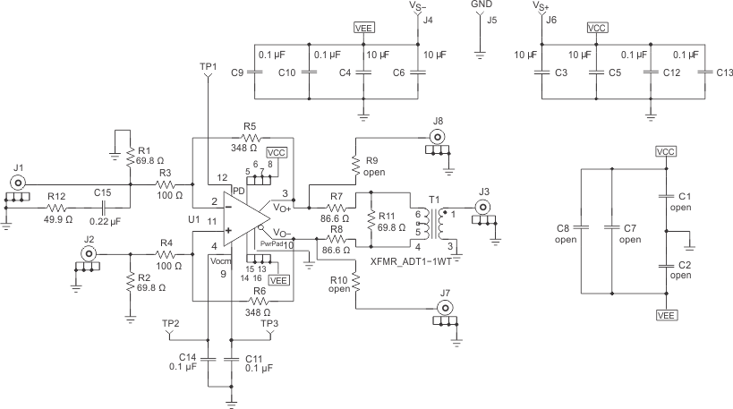
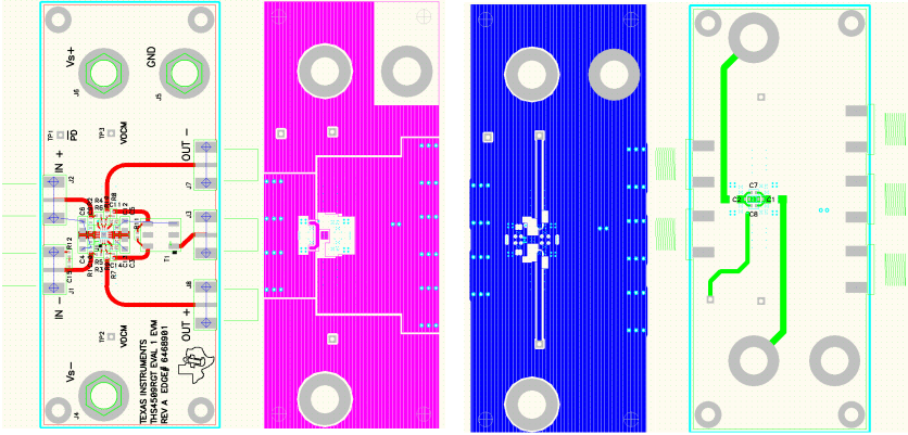
Figure 93 is the THS4509 EVAL1 EVM schematic; layers 1 through 4 of the PCB are shown Figure 94.
 Figure 93. THS4509 EVAL1 EVM Schematic
 Figure 94. THS4509 EVAL1 EVM Layer 1 Through Layer 4
11.3 PowerPAD™ Design Considerations
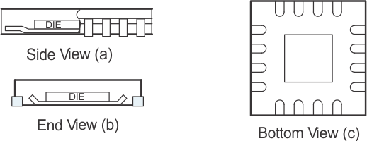
The THS4509 is available in a thermally-enhanced PowerPAD family of packages. These packages are constructed using a downset leadframe on which the die is mounted (see Figure 95a and Figure 95b). This arrangement results in the lead frame being exposed as a thermal pad on the underside of the package (see Figure 95c). Because this thermal pad has direct thermal contact with the die, excellent thermal performance can be achieved by providing a good thermal path away from the thermal pad.
NOTE
The THS4509 has no electrical connection between the PowerPAD and circuitry on the die. Connecting the PowerPAD to any potential voltage between VS+ and VS– is acceptable. It is most important that it be connected for maximum heat dissipation.
The PowerPAD package allows both assembly and thermal management in one manufacturing operation.
During the surface-mount solder operation (when the leads are being soldered), the thermal pad can also be soldered to a copper area underneath the package. Through the use of thermal paths within this copper area, heat can be conducted away from the package into either a ground plane or other heat dissipating device.
The PowerPAD package represents a breakthrough in combining the small area and ease of assembly of surface-mount with the previously awkward mechanical methods of heatsinking.
 Figure 95. Views of Thermally-Enhanced Package