SNVA870A March 2019 – April 2020 LM25143 , LM25143-Q1 , LM5143 , LM5143-Q1 , LM5143A-Q1
6.3 PCB Layout
Figure 6 through show the design using a 6-layer PCB with 2-oz copper thickness. The design is essentially a single-sided design except for certain input filtering and small-signal components located on the bottom side.
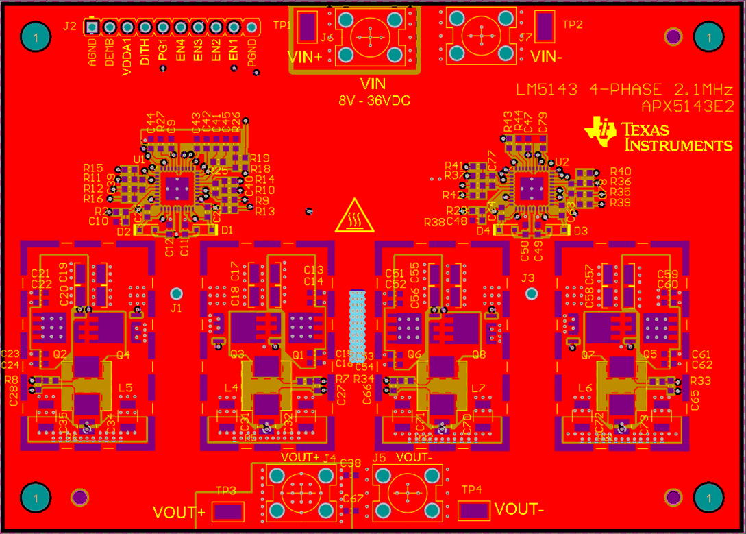 Figure 6. Top Copper (Top View)
 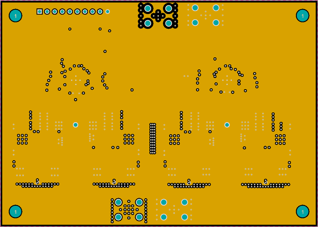 Figure 7. Layer 2 Copper (Top View)
 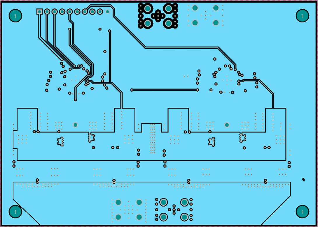 Figure 8. Layer 3 Copper (Top View)
 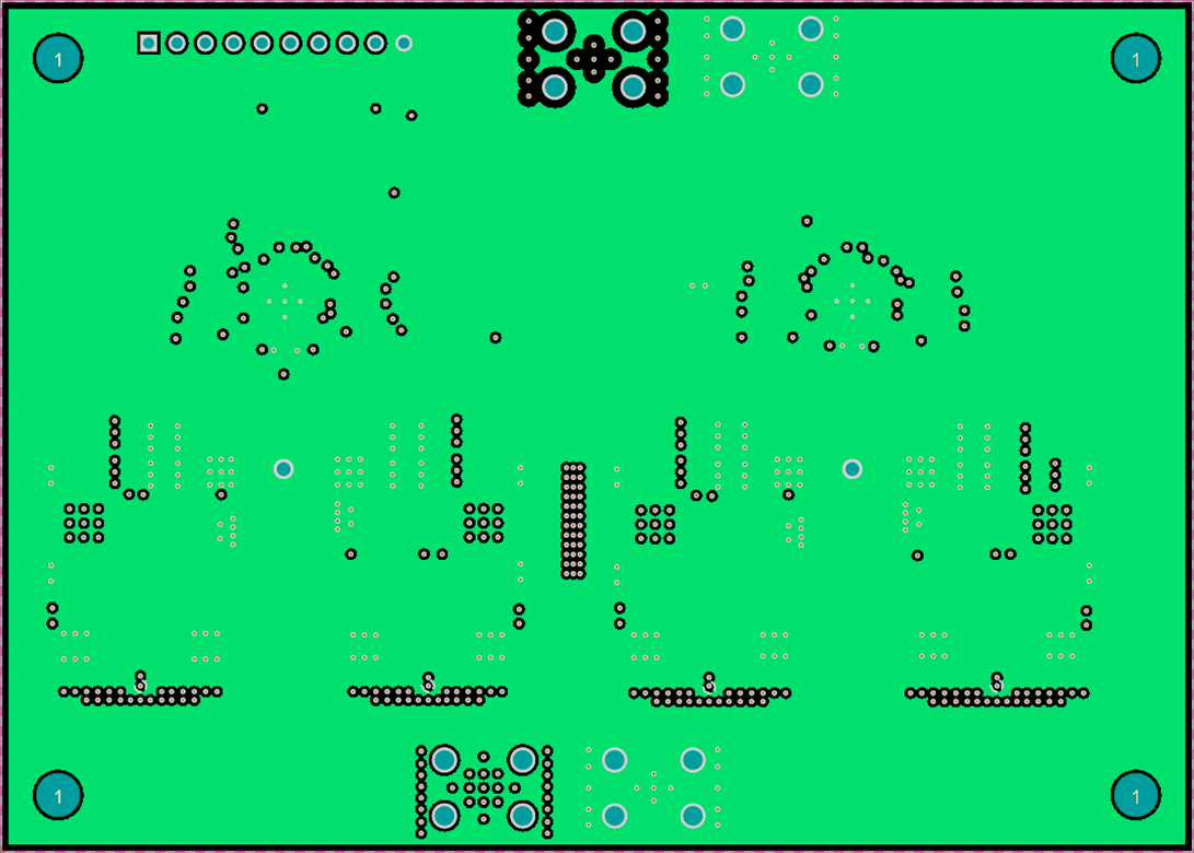 Figure 9. Layer 4 Copper (Top View)
 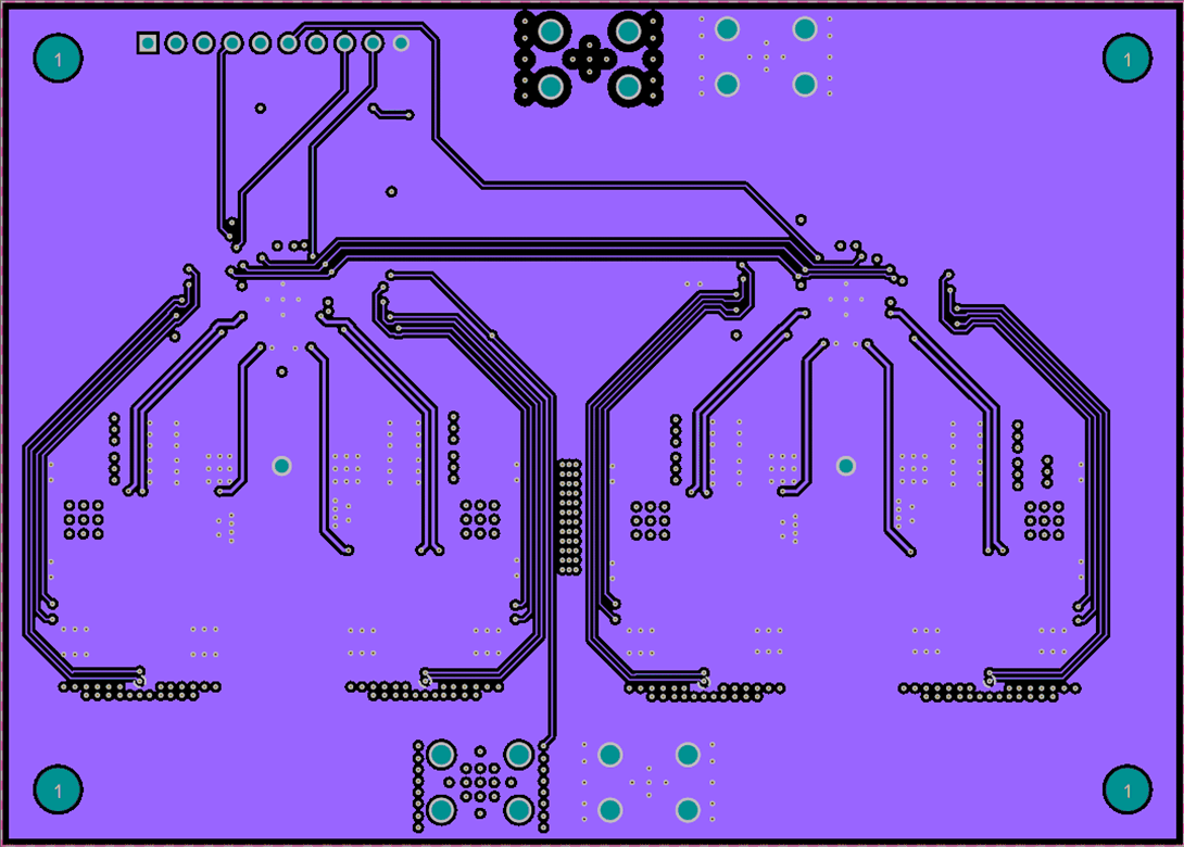 Figure 10. Layer 5 Copper (Top View)
 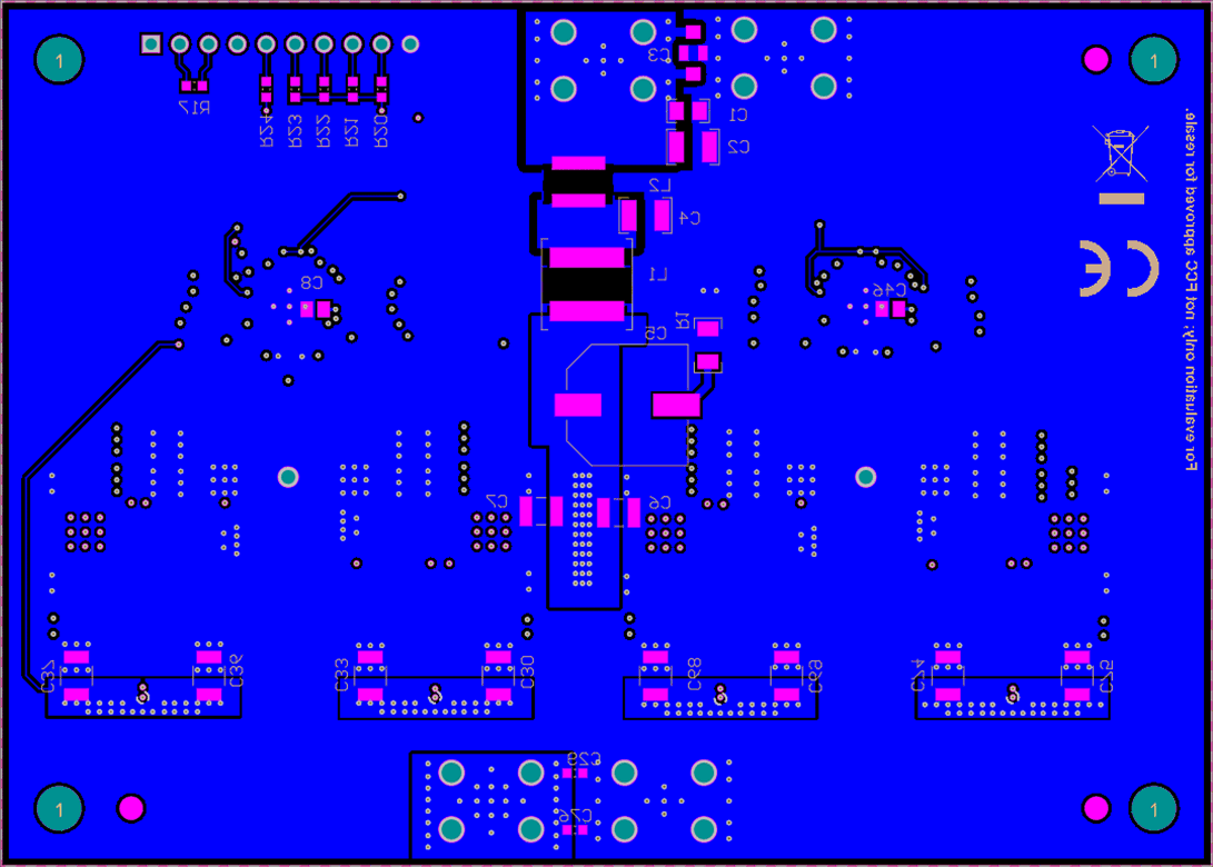 Figure 11. Bottom Copper (Top View)