SLVUDF9 October 2025 TRF3302
3.1 Schematics
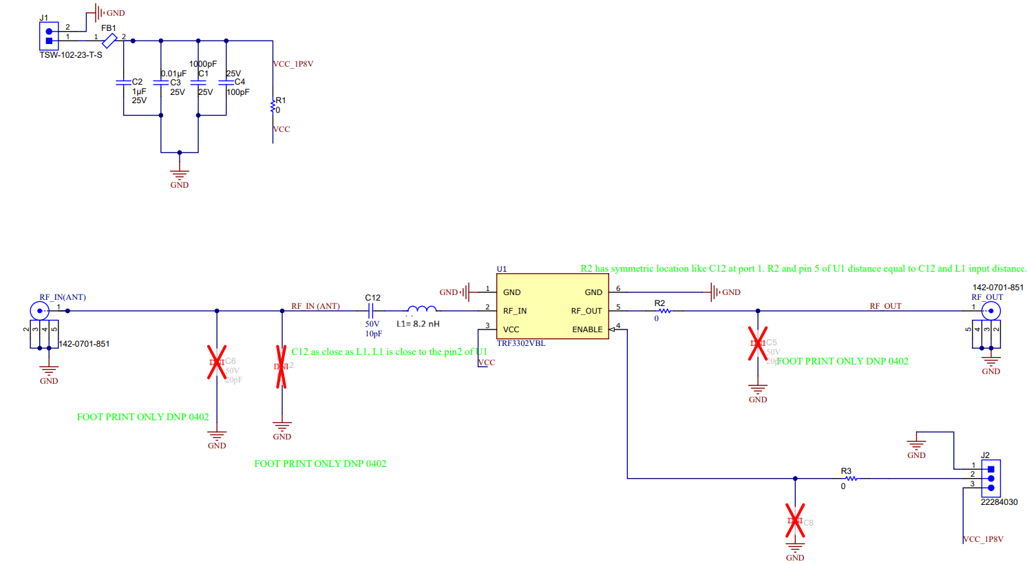
Figure 3-1 shows the EVM schematic.
- FB1, C2 and C3 are optional in the BOM. FB1 can be replaced by 0ohm 0201 resistor is sufficient for the DC operation of the TRF3302.
- The EVM has input capacitor C12 installed for DC blocking and RF signal coupling while L1 inductor is tuned to support 1300 to 1630MHz (L1 band) by default.
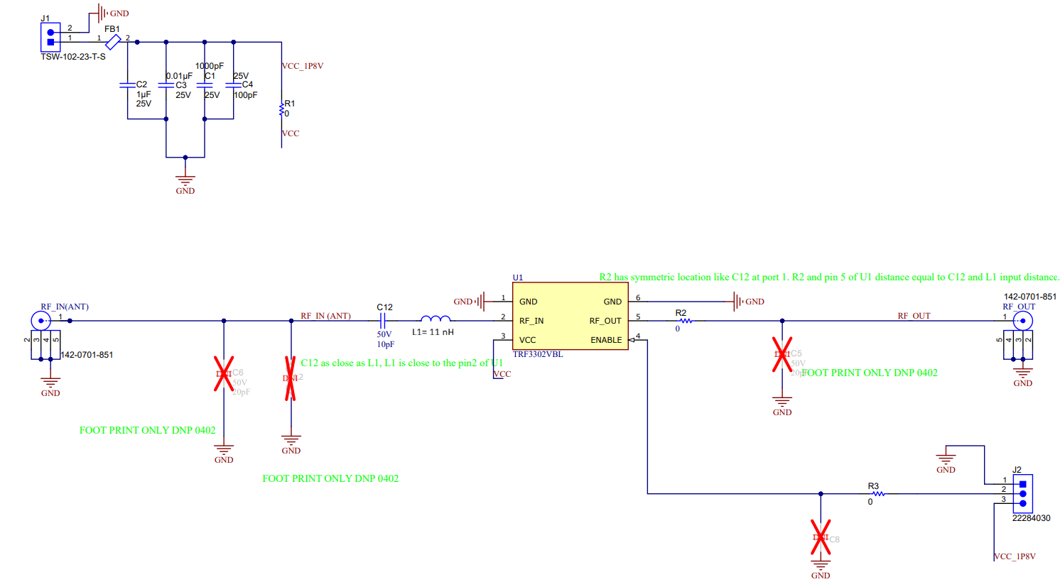
- Additional three L1 = 11nH inductors are provided with the EVM kit to replace L1 and optimize the TRF3302 to support 1165 to 1320MHz (L2/L5 band) as shown in Figure 3-2.
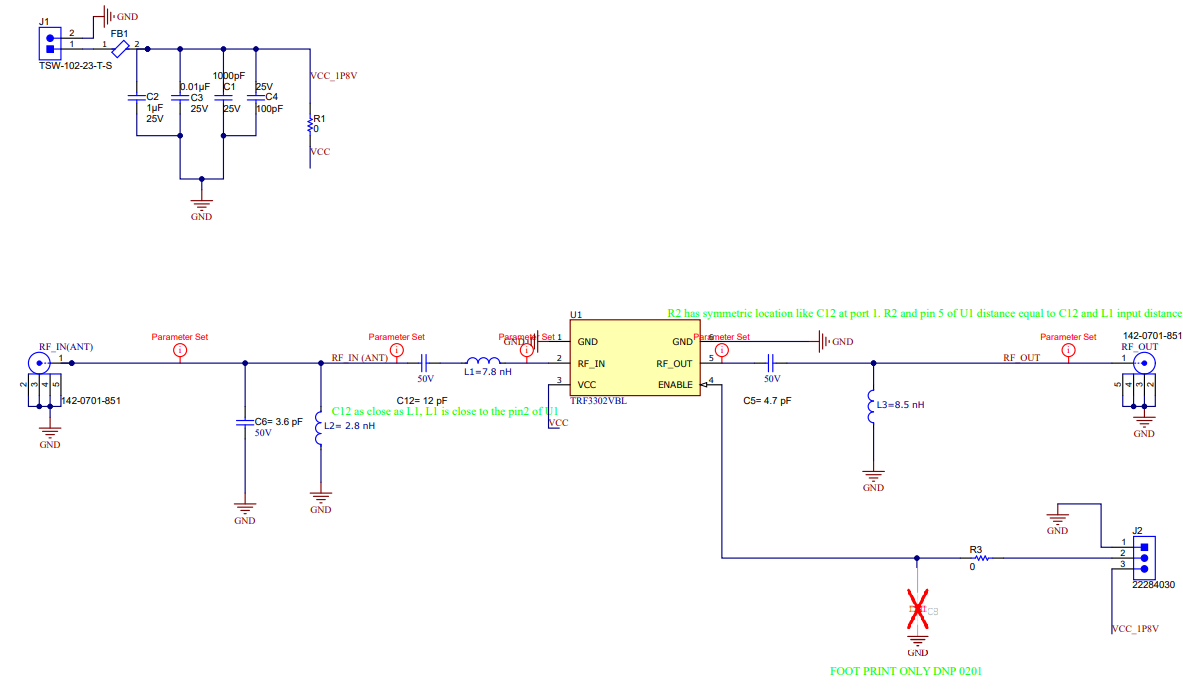
- Replace C6, C12, L1, and L2 with 3.6pF, 12pF, 7.8nH and 2.8nH to optimize performance across 1165 to 1630MHz (all GPS/GNSS bands) as shown in Figure 3-3. R2 has to be replaced with capacitor value 4.7pF and C5 has to be replaced with inductor value 8.5nH to achieve gain flatness and a slight improvement in output matching.
 Figure 3-1 TRF3302EVM Schematic for L1 Band
  Figure 3-2 TRF3302EVM Schematic for L2/L5 Bands
 Figure 3-3 TRF3302EVM Schematic for All GPS/GNSS Bands