ZHCSFK9C September 2016 – October 2024 UCC28950-Q1 , UCC28951-Q1
PRODUCTION DATA
- 1
- 1 特性
- 2 應(yīng)用
- 3 說(shuō)明
- 4 Pin Configuration and Functions
- 5 Specifications
-
6 Detailed Description
- 6.1 Overview
- 6.2 Functional Block Diagram
- 6.3
Feature Description
- 6.3.1 Start-Up Protection Logic
- 6.3.2 Voltage Reference (VREF)
- 6.3.3 Error Amplifier (EA+, EA–, COMP)
- 6.3.4 Soft-Start and Enable (SS/EN)
- 6.3.5 Light-Load Power Saving Features
- 6.3.6 Adaptive Delay, (Delay Between OUTA and OUTB, OUTC and OUTD (DELAB, DELCD, ADEL))
- 6.3.7 Adaptive Delay (Delay Between OUTA and OUTF, OUTB and OUTE (DELEF, ADELEF)
- 6.3.8 Minimum Pulse (TMIN)
- 6.3.9 Burst Mode
- 6.3.10 Switching Frequency Setting
- 6.3.11 Slope Compensation (RSUM)
- 6.3.12 Dynamic SR ON/OFF Control (DCM Mode)
- 6.3.13 Current Sensing (CS)
- 6.3.14 Cycle-by-Cycle Current Limit Current Protection and Hiccup Mode
- 6.3.15 Synchronization (SYNC)
- 6.3.16 Outputs (OUTA, OUTB, OUTC, OUTD, OUTE, OUTF)
- 6.3.17 Supply Voltage (VDD)
- 6.3.18 Ground (GND)
- 6.4 Device Functional Modes
-
7 Application and Implementation
- 7.1 Application Information
- 7.2
Typical Application
- 7.2.1 Design Requirements
- 7.2.2
Detailed Design Procedure
- 7.2.2.1 Power Loss Budget
- 7.2.2.2 Preliminary Transformer Calculations (T1)
- 7.2.2.3 QA, QB, QC, QD FET Selection
- 7.2.2.4 Selecting LS
- 7.2.2.5 Selecting Diodes DB and DC
- 7.2.2.6 Output Inductor Selection (LOUT)
- 7.2.2.7 Output Capacitance (COUT)
- 7.2.2.8 Select FETs QE and QF
- 7.2.2.9 Input Capacitance (CIN)
- 7.2.2.10 Current Sense Network (CT, RCS, R7, DA)
- 7.2.3 Application Curves
- 7.3 Power Supply Recommendations
- 7.4 Layout
- 8 Device and Documentation Support
- 9 Revision History
- 10Mechanical, Packaging, and Orderable Information
封裝選項(xiàng)
機(jī)械數(shù)據(jù) (封裝 | 引腳)
- PW|24
散熱焊盤(pán)機(jī)械數(shù)據(jù) (封裝 | 引腳)
訂購(gòu)信息
7.2.2.10 Current Sense Network (CT, RCS, R7, DA)
The CT chosen for this design has a turns ratio (CTRAT) of 100:1 in Equation 97:

Calculate nominal peak current (IP1) at VINMIN:
The peak primary current is calculated using Equation 98:

The CS pin voltage where peak current limit will trip is:

Calculate current sense resistor (RCS) and leave 300mV for slope compensation using Equation 100. Include a 1.1 factor for margin:
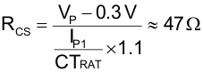
Select a standard resistor for RCS:

Estimate the power loss for RCS using Equation 102:

Calculate maximum reverse voltage (VDA) on DA using Equation 103:

Estimate the DA power loss (PDA) using Equation 104:

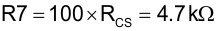
Calculate reset resistor R7:
Resistor R7 is used to reset the current sense transformer CT:
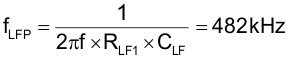
Resistor RLF1 and capacitor CLF form a low-pass filter for the current sense signal (Pin 15). For this design, chose the following values. This filter has a low frequency pole (fLFP) at 482kHz, (which is appropriate for most applications) but may be adjusted to suit individual layouts and EMI present in the design.


The UCC2895x-Q1 VREF output (Pin 1) needs a high frequency bypass capacitor to filter out high frequency noise. This pin needs at least 1μF of high-frequency bypass capacitance (CREF).

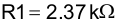
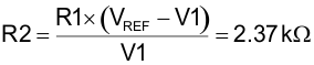
The voltage amplifier reference voltage (Pin 2, EA +) can be set with a voltage divider (R1, R2), for this design example, the error amplifier reference voltage (V1) will be set to 2.5V. Select a standard resistor value for R1 and then calculate resistor value R2.
UCC2895x-Q1 reference voltage:

Set voltage amplifier reference voltage:

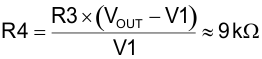
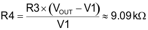
The voltage divider formed by resistor R3 and R4 are chosen to set the DC output voltage (VOUT) at Pin 3 (EA-).
Select a standard resistor for R3:

Calculate R4 using Equation 115:
Then choose a standard resistor for R4 using Equation 116:
TI recommends using an RCD clamp to protect the output synchronous FETs from overvoltage due to switch node ringing.
 Figure 7-5 Daughter
Board Schematic
Figure 7-5 Daughter
Board Schematic