ZHCSBM1D September 2013 – August 2024 TS3USB3031
PRODUCTION DATA
- 1
- 1 特性
- 2 應(yīng)用
- 3 說(shuō)明
- 4 Pin Configuration and Functions
- 5 Specifications
- Parameter Measurement Information
- 6 Detailed Description
- 7 Application and Implementation
- 8 Device and Documentation Support
- 9 Revision History
- 10Mechanical, Packaging, and Orderable Information
封裝選項(xiàng)
機(jī)械數(shù)據(jù) (封裝 | 引腳)
- RMG|12
散熱焊盤機(jī)械數(shù)據(jù) (封裝 | 引腳)
訂購(gòu)信息
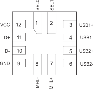
4 Pin Configuration and Functions
 Figure 4-1 RMG Package, 12-Pin VQFN
(Top View)
 Figure 4-2 RMG Package, 12-Pin VQFN
(Bottom View)
Figure 4-2 RMG Package, 12-Pin VQFN
(Bottom View)Table 4-1 Pin Functions
| PIN | TYPE(1) | DESCRIPTION | |
|---|---|---|---|
| NAME | NO. | ||
| SEL0 | 1 | I | Digital control Input |
| SEL1 | 2 | I | Digital control Input |
| USB1+ | 3 | I/O | Differential signal path 1 |
| USB1– | 4 | I/O | Differential signal path 1 |
| USB2+ | 5 | I/O | Differential signal path 2 |
| USB2– | 6 | I/O | Differential signal path 2 |
| MHL+ | 7 | I/O | Differential signal path 3 |
| MHL– | 8 | I/O | Differential signal path 3 |
| GND | 9 | G | Ground |
| D– | 10 | I/O | Common Differential signal path |
| D+ | 11 | I/O | Common Differential signal path |
| VCC | 12 | P | Power Supply |
(1) G = Ground, I = Input, O = Output, P = Power