ZHCSAQ2B January 2013 – April 2017 TS3A5223
PRODUCTION DATA.
- 1 特性
- 2 應用
- 3 說明
- 4 修訂歷史記錄
- 5 Pin Configuration and Functions
- 6 Specifications
- 7 Parameter Measurement Information
- 8 Detailed Description
- 9 Application and Implementation
- 10Power Supply Recommendations
- 11Layout
- 12器件和文檔支持
- 13機械、封裝和可訂購信息
封裝選項
機械數(shù)據(jù) (封裝 | 引腳)
- RSW|10
散熱焊盤機械數(shù)據(jù) (封裝 | 引腳)
訂購信息
6 Specifications
6.1 Absolute Maximum Ratings(1)
Specified at TA= –40°C to 85°C unless otherwise noted.| VALUE | UNIT | ||||
|---|---|---|---|---|---|
| MIN | MAX | ||||
| VCC | Positive DC supply voltage | –0.3 | 4.3(2) | V | |
| VCOM
VNO VNC |
Analog voltage | –0.3 | 4.3(2) | V | |
| ICOM
INO INC |
On-state switch continuous current | ±300 | mA | ||
| ICOM
INO INC |
On-state switch peak current (1ms pulse at 10% duty cycle) | ±500 | mA | ||
| PD | Total device power dissipation at TA = 85°C |
10-µQFN RSW | 430 | mW | |
| TA | Operating free-air ambient temperature range | –40 | 85 | °C | |
| TJ | Junction temperature range | –55 | 150 | °C | |
| Tstg | Storage temperature range | –55 | 150 | °C | |
(1) Stresses beyond those listed under "Absolute Maximum Ratings" may cause permanent damage to the device. These are stress ratings only and functional operation of the device at these conditions is not implied. Exposure to absolute-maximum-rated conditions for extended periods may affect device reliability.
(2) Not rated for continuous operation, 0.5% duty cycle at 1 kHz recommended
6.2 ESD Ratings
| VALUE | UNIT | |||
|---|---|---|---|---|
| V(ESD) | Electrostatic discharge | Human-body model (HBM), per ANSI/ESDA/JEDEC JS-001(1) | ±2000 | V |
| Charged-device model (CDM), per JEDEC specification JESD22-C101(2) | ±500 | |||
(1) JEDEC document JEP155 states that 500-V HBM allows safe manufacturing with a standard ESD control process.
(2) JEDEC document JEP157 states that 250-V CDM allows safe manufacturing with a standard ESD control process.
6.3 Recommended Operating Conditions
over operating free-air temperature range (unless otherwise noted)| MIN | MAX | UNIT | |||
|---|---|---|---|---|---|
| VCC | Positive DC supply voltage | 1.65 | 3.6 | V | |
| VCOM, VNO, VNC | Analog voltage range | 0 | VCC | V | |
| VSEL1
VSEL2 |
Digital logic voltage | 0 | VCC | V | |
| TA | Operating free-air ambient temperature range | –40 | 85 | ºC | |
6.4 Thermal Information
| THERMAL METRIC(1) | TS3A5223 | UNIT | |
|---|---|---|---|
| RSW (UQFN) | |||
| 10 PINS | |||
| RθJA | Junction-to-ambient thermal resistance | 92.5 | °C/W |
| RθJC(top) | Junction-to-case (top) thermal resistance | 46.0 | °C/W |
| RθJB | Junction-to-board thermal resistance | 44.5 | °C/W |
| ψJT | Junction-to-top characterization parameter | 1.5 | °C/W |
| ψJB | Junction-to-board characterization parameter | 44.5 | °C/W |
| RθJC(bot) | Junction-to-case (bottom) thermal resistance | 31.2 | °C/W |
(1) For more information about traditional and new thermal metrics, see the Semiconductor and IC Package Thermal Metrics application report.
6.5 Electrical Characteristics
Specified over the recommended junction temperature range TA = TJ = –40°C to 85°C Typical values are at TA= TJ = 25°C (unless otherwise noted).| PARAMETER | VCC (V) | TEST CONDITIONS | MIN | TYP | MAX | UNIT | |
|---|---|---|---|---|---|---|---|
| DC CHARACTERISTICS | |||||||
| VIH | High-level Input voltage SEL1, SEL2 inputs | 3.6 | 0.8 | V | |||
| 2.3 | 0.8 | ||||||
| 1.8 | 0.8 | ||||||
| VIL | Low-level Input voltage SEL1, SEL2 inputs | 3.6 | 0.3 | V | |||
| 2.3 | 0.3 | ||||||
| 1.8 | 0.3 | ||||||
| RON | Switch ON Resistance | 3.6 | VS = 0 to VCC, IS = 100 mA, VSEL = 1 V, 0 V |
0.45 | 0.6 | Ω | |
| 2.3 | 0.6 | 0.8 | |||||
| 1.8 | 0.85 | 1.2 | |||||
| ΔRON | Difference of on-state resistance between switches | 3.6 | VS = 2 V, 0.8 V, IS = 100 mA, VSEL = 1 V, 0 V |
0.05 | Ω | ||
| RON-FLAT | ON resistance flatness | 3.6 | VS = 0 to VCC, IS = 100mA, VSEL = 1 V, 0 V |
0.1 | 0.2 | Ω | |
| 2.3 | 0.15 | 0.35 | |||||
| 1.8 | 0.4 | 0.65 | |||||
| IOFF | NC, NO pin leakage current when switch is off | 3.6 | VS = 0.3 or 3.0V, VCOM = 3 or 0.3 V | 5 | 90 | nA | |
| IS(ON) | NC, NO pin leakage current when switch is on | 3.6 | VS = 0.3 or 3.0V, VCOM = No Load | 4 | 60 | nA | |
| ISEL | Select pin input leakage current | VS | VS = 0 or 3.6 V | 100 | nA | ||
| ICC | Quiescent supply current | 3.6 | VSEL = 0 or VCC | 700 | 2000 | nA | |
| ICCLV | Supply current change | 3.6 | VSEL = 1 V to VSEL = VCC | 200 | nA | ||
| SWITCHING PARAMETERS(1)(2) | |||||||
| tPHL | Logic high to low propagation delay | 3.6 | RL = 50 Ω, CL = 35 pF | 0.1 | ns | ||
| 2.5 | 0.2 | ||||||
| 1.8 | 0.2 | ||||||
| tPLH | Logic low to high propagation delay | 3.6 | RL = 50 Ω, CL = 35 pF | 0.1 | ns | ||
| 2.5 | 0.2 | ||||||
| 1.8 | 0.2 | ||||||
| tON | Turn-ON time | 2.3 - 3.6 | RL = 50 Ω, CL = 35 pF, VS = 1.5 V | 70 | ns | ||
| tOFF | Turn-OFF time | 2.3 - 3.6 | RL = 50 Ω, CL = 35 pF, VS = 1.5 V | 75 | ns | ||
| tBBM | Break-before-make time delay | 3.6 | RL = 50 Ω, CL = 35 pF, VS = 1.5 V | 2 | 8 | ns | |
| QINJ | Charge Injection | 3.6 | CL = 1 nF, VS = 0 V | 40 | pC | ||
| AC CHARACTERISTICS | |||||||
| BW | -3 dB Bandwidth | 1.65 - 3.6 | RL = 50 Ω, CL = 35 pF | 80 | MHz | ||
| VISO | Channel OFF isolation | 1.65 - 3.6 | VS = 1 Vrms, f = 100 kHz | –70 | dB | ||
| VXtalk | Channel-to-Channel Crosstalk | 1.65 - 3.6 | VS = 1 Vrms, f = 100kHz | –75 | dB | ||
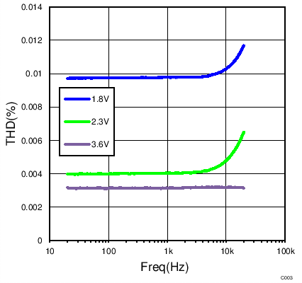
| THD | Total harmonic distortion | 1.65 - 3.6 | RL = 600 Ω, VSEL = 2 Vpk-pk, f = 20 Hz to 20 kHz |
0.01% | |||
| CSEL | Select pin input capacitance | 3.3 | f = 1 MHz | 3 | pF | ||
| CON | NC, NO, and COM input capacitance when switch is on | 3.3 | f = 1 MHz | 115 | pF | ||
| COFF | NC, NO, and COM input capacitance when switch is off | 3.3 | f = 1 MHz | 50 | pF | ||
(1) Rise and Fall propagation delays, tPHL and tPLH, are measured between 50% values of the input and the corresponding output signal amplitude transition.
(2) Specified by characterization only. Validated during qualification. Not measured in production testing.
6.6 Typical Characteristics
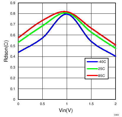
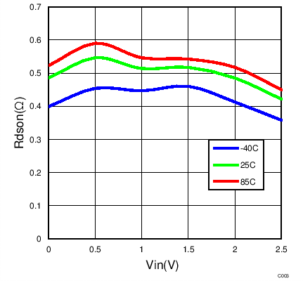
| VCC = 1.8 V |
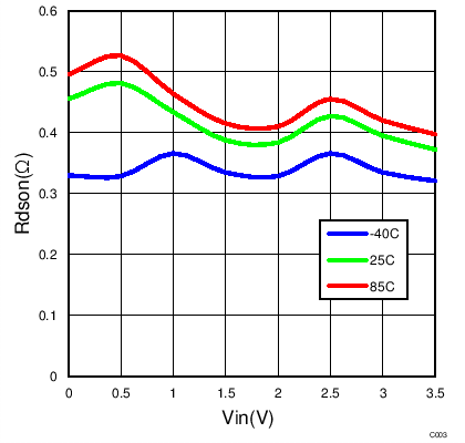
| VCC = 3 V |
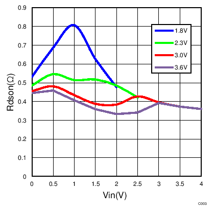
| TA = 25°C |
| VCC = 2.3 V |
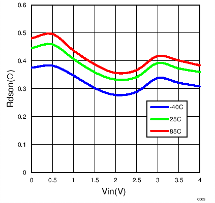
| VCC = 3.6 V |
