SLUS791A July 2007 – September 2015 TPS28226
PRODUCTION DATA.
- 1 Features
- 2 Applications
- 3 Description
- 4 Revision History
- 5 Pin Configuration and Functions
- 6 Specifications
- 7 Detailed Description
- 8 Application and Implementation
- 9 Power Supply Recommendations
- 10Layout
- 11Device and Documentation Support
- 12Mechanical, Packaging, and Orderable Information
封裝選項(xiàng)
機(jī)械數(shù)據(jù) (封裝 | 引腳)
散熱焊盤機(jī)械數(shù)據(jù) (封裝 | 引腳)
- DRB|8
訂購(gòu)信息
10 Layout
10.1 Layout Guidelines
To improve the switching characteristics and efficiency of a design, the following layout rules need to be followed.
- Locate the driver as close as possible to the MOSFETs.
- Locate the VDD and bootstrap capacitors as close as possible to the driver.
- Pay special attention to the GND trace. Use the thermal pad of the DFN-8 package as the GND by connecting it to the GND pin. The GND trace or pad from the driver goes directly to the source of the MOSFET but should not include the high current path of the main current flowing through the drain and source of the MOSFET.
- Use a similar rule for the PHASE node as for the GND.
- Use wide traces for UGATE and LGATE closely following the related PHASE and GND traces. Eighty to 100 mils width is preferable where possible.
- Use at least 2 or more vias if the MOSFET driving trace needs to be routed from one layer to another. For the GND the number of vias are determined not only by the parasitic inductance but also by the requirements for the thermal pad.
- Avoid PWM and enable traces going close to the PHASE node and pad where high dV/dT voltage can induce significant noise into the relatively high impedance leads.
It should be taken into account that poor layout can cause 3% to 5% less efficiency versus a good layout design and can even decrease the reliability of the whole system.
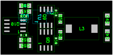
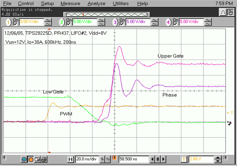
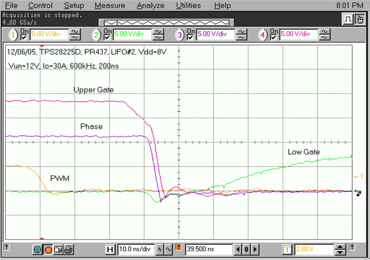
The schematic of one of the phases in a multi-phase synchronous buck regulator and the related layout are shown in Figure 25 and Figure 41. These help to illustrate good design practices. The power stage includes one high-side MOSFET Q10 and two low-side MOSFETS (Q8 and Q9). The driver (U7) is located on bottom side of PCB close to the power MOSFETs. The related switching waveforms during turning ON and OFF of upper FET are shown in Figure 39 and Figure 40. The dead time during turning ON is only 10 ns (Figure 39) and 22 ns during turning OFF (Figure 40).
10.2 Layout Example
 Figure 41. Component Placement Based on Schematic in Figure 25

