SCPS164D MAY 2007 – February 2017 TCA6507
PRODUCTION DATA.
- 1 Features
- 2 Applications
- 3 Description
- 4 Revision History
- 5 Pin Configuration and Functions
- 6 Specifications
- 7 Parameter Measurement Information
-
8 Detailed Description
- 8.1 Overview
- 8.2 Functional Block Diagram
- 8.3 Feature Description
- 8.4 Device Functional Modes
- 8.5 Programming
- 8.6
Register Maps
- 8.6.1 Registers 0x00 - 0x02 (Select Registers)
- 8.6.2 Register 0x03 (Fade-ON Time)
- 8.6.3 Register 0x04 (Fully-ON Time)
- 8.6.4 Register 0x05 (Fade-OFF Time)
- 8.6.5 Register 0x06 - 0x07 (Fully-OFF Time)
- 8.6.6 Register 0x08 (Maximum Intensity per Bank)
- 8.6.7 Register 0x09 (One-Shot / Master Intensity)
- 8.6.8 Register 0x0A (Initialization Register)
- 9 Application and Implementation
- 10Power Supply Recommendations
- 11Layout
- 12Device and Documentation Support
- 13Mechanical, Packaging, and Orderable Information
封裝選項(xiàng)
機(jī)械數(shù)據(jù) (封裝 | 引腳)
散熱焊盤機(jī)械數(shù)據(jù) (封裝 | 引腳)
- RUE|12
訂購(gòu)信息
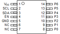
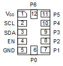
5 Pin Configuration and Functions
PW Package
14-Pin TSSOP
Top View

RUE Package
12-Pin X2QFN
Top View

Pin Functions –TSSOP and X2QFN
| PIN | I/O | DESCRIPTION | ||
|---|---|---|---|---|
| NAME | NO. | |||
| PW | RUE | |||
| EN | 4 | 4 | I | Enable input. If set to low, it puts the TCA6507 in shutdown mode and resets the internal registers and I2C/SMBus state machine to their default states |
| GND | 5 | 5 | — | Ground |
| P0 | 8 | 6 | O | P-port output 0. Open-drain design structure |
| P1 | 9 | 7 | O | P-port output 1. Open-drain design structure |
| P2 | 10 | 8 | O | P-port output 2. Open-drain design structure |
| P3 | 11 | 9 | O | P-port output 3. Open-drain design structure |
| P4 | 12 | 10 | O | P-port output 4. Open-drain design structure |
| P5 | 13 | 11 | O | P-port output 5. Open-drain design structure |
| P6 | 14 | 12 | O | P-port output 6. Open-drain design structure |
| SDA | 3 | 3 | I/O | Serial data bus. Connect to VCC through a pull-up resistor |
| SCL | 2 | 2 | I | Serial clock bus. Connect to VCC through a pull-up resistor |
| VCC | 1 | 1 | — | Supply voltage of I2C registers, oscillator, and control logic. Connect directly to VCC of the external I2C master. Provides voltage-level translation |
ZXU Package
12-Pin BGA MICROSTAR JUNIOR
Top View

Table 1. ZXU Package Terminal Assignments
| C | B | A | |
|---|---|---|---|
| 1 | P1 | P2 | GND |
| 2 | P3 | EN | SDA |
| 3 | P4 | P0 | SCL |
| 4 | P5 | P6 | VCC |
Pin Functions –BGA Microstar Junior
| PIN | I/O | DESCRIPTION | |
|---|---|---|---|
| NO. | NAME | ||
| A1 | GND | — | Ground |
| A2 | SDA | I/O | Serial data bus. Connect to VCC through a pullup resistor |
| A3 | SCL | I | Serial clock bus. Connect to VCC through a pullup resistor |
| A4 | VCC | — | Supply voltage of I2C registers, oscillator, and control logic. Connect directly to VCC of the external I2C master. Provides voltage-level translation |
| B1 | P2 | O | P-port output 2. Open-drain design structure |
| B2 | EN | I | Enable input. If set to low, it puts the TCA6507 in shutdown mode and resets the internal registers and I2C/SMBus state machine to their default states |
| B3 | P0 | O | P-port output 0. Open-drain design structure |
| B4 | P6 | O | P-port output 6. Open-drain design structure |
| C1 | P1 | O | P-port output 1. Open-drain design structure |
| C2 | P3 | O | P-port output 3. Open-drain design structure |
| C3 | P4 | O | P-port output 4. Open-drain design structure |
| C4 | P5 | O | P-port output 5. Open-drain design structure |