ZHCSEB9A October 2015 – November 2015 LMK61PD0A2
PRODUCTION DATA.
- 1 特性
- 2 應(yīng)用
- 3 說明
- 4 修訂歷史記錄
- 5 Device Control
- 6 Pin Configuration and Functions
-
7 Specifications
- 7.1 Absolute Maximum Ratings
- 7.2 ESD Ratings
- 7.3 Recommended Operating Conditions
- 7.4 Thermal Information
- 7.5 Electrical Characteristics - Power Supply
- 7.6 LVPECL Output Characteristics
- 7.7 LVDS Output Characteristics
- 7.8 HCSL Output Characteristics
- 7.9 OE Input Characteristics
- 7.10 OS, FS[1:0] Input Characteristics
- 7.11 Frequency Tolerance Characteristics
- 7.12 Power-On/Reset Characteristics (VDD)
- 7.13 PSRR Characteristics
- 7.14 PLL Clock Output Jitter Characteristics
- 7.15 Additional Reliability and Qualification
- 7.16 Typical Performance Characteristics
- 8 Parameter Measurement Information
- 9 Detailed Description
- 10Application and Implementation
- 11Power Supply Recommendations
- 12Layout
- 13器件和文檔支持
- 14機(jī)械、封裝和可訂購信息
封裝選項(xiàng)
機(jī)械數(shù)據(jù) (封裝 | 引腳)
- SIA|8
散熱焊盤機(jī)械數(shù)據(jù) (封裝 | 引腳)
訂購信息
8 Parameter Measurement Information
8.1 Device Output Configurations
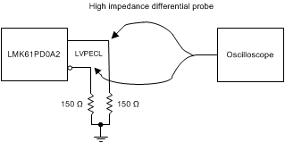
 Figure 7. LVPECL Output DC Configuration during Device Test
 Figure 8. LVDS Output DC Configuration during Device Test
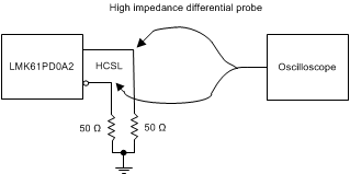
 Figure 9. HCSL Output DC Configuration during Device Test
 Figure 10. LVPECL Output AC Configuration during Device Test
 Figure 11. LVDS Output AC Configuration during Device Test
 Figure 12. HCSL Output AC Configuration during Device Test
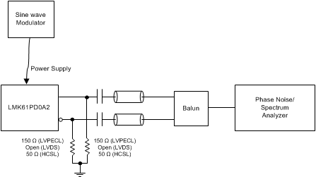
 Figure 13. PSRR Test Setup
 Figure 14. Differential Output Voltage and Rise/Fall Time