ZHCS558H June 2011 – July 2014 LM5066
PRODUCTION DATA.
- 1 特性
- 2 應(yīng)用
- 3 說(shuō)明
- 4 簡(jiǎn)化電路原理圖
- 5 修訂歷史記錄
- 6 Device Comparison Table
- 7 Pin Configuration and Functions
- 8 Specifications
-
9 Detailed Description
- 9.1 Overview
- 9.2 Functional Block Diagram
- 9.3 Feature Description
- 9.4 Device Functional Modes
- 9.5
Programming
- 9.5.1 PMBus Command Support
- 9.5.2
Standard PMBus Commands
- 9.5.2.1 OPERATION (01h)
- 9.5.2.2 CLEAR_FAULTS (03h)
- 9.5.2.3 CAPABILITY (19h)
- 9.5.2.4 VOUT_UV_WARN_LIMIT (43h)
- 9.5.2.5 OT_FAULT_LIMIT (4Fh)
- 9.5.2.6 OT_WARN_LIMIT (51h)
- 9.5.2.7 VIN_OV_WARN_LIMIT (57h)
- 9.5.2.8 VIN_UV_WARN_LIMIT (58h)
- 9.5.2.9 STATUS_BYTE (78h)
- 9.5.2.10 STATUS_WORD (79h)
- 9.5.2.11 STATUS_VOUT (7Ah)
- 9.5.2.12 STATUS_INPUT (7Ch)
- 9.5.2.13 STATUS_TEMPERATURE (7dh)
- 9.5.2.14 STATUS_CML (7Eh)
- 9.5.2.15 STATUS_MFR_SPECIFIC (80h)
- 9.5.2.16 READ_VIN (88h)
- 9.5.2.17 READ_VOUT (8Bh)
- 9.5.2.18 READ_TEMPERATURE_1 (8Dh)
- 9.5.2.19 MFR_ID (99h)
- 9.5.2.20 MFR_MODEL (9Ah)
- 9.5.2.21 MFR_REVISION (9Bh)
- 9.5.3
Manufacturer Specific PMBus Commands
- 9.5.3.1 MFR_SPECIFIC_00: READ_VAUX (D0h)
- 9.5.3.2 MFR_SPECIFIC_01: MFR_READ_IIN (D1h)
- 9.5.3.3 MFR_SPECIFIC_02: MFR_READ_PIN (D2h)
- 9.5.3.4 MFR_SPECIFIC_03: MFR_IN_OC_WARN_LIMIT (D3h)
- 9.5.3.5 MFR_SPECIFIC_04: MFR_PIN_OP_WARN_LIMIT (D4h)
- 9.5.3.6 MFR_SPECIFIC_05: READ_PIN_PEAK (D5h)
- 9.5.3.7 MFR_SPECIFIC_06: CLEAR_PIN_PEAK (D6h)
- 9.5.3.8 MFR_SPECIFIC_07: GATE_MASK (D7h)
- 9.5.3.9 MFR_SPECIFIC_08: ALERT_MASK (D8h)
- 9.5.3.10 MFR_SPECIFIC_09: DEVICE_SETUP (D9h)
- 9.5.3.11 MFR_SPECIFIC_10: BLOCK_READ (DAh)
- 9.5.3.12 MFR_SPECIFIC_11: SAMPLES_FOR_AVG (DBh)
- 9.5.3.13 MFR_SPECIFIC_12: READ_AVG_VIN (DCh)
- 9.5.3.14 MFR_SPECIFIC_13: READ_AVG_VOUT (DDh)
- 9.5.3.15 MFR_SPECIFIC_14: READ_AVG_IIN (DEh)
- 9.5.3.16 MFR_SPECIFIC_15: READ_AVG_PIN
- 9.5.3.17 MFR_SPECIFIC_16: BLACK_BOX_READ (E0h)
- 9.5.3.18 MFR_SPECIFIC_17: READ_DIAGNOSTIC_WORD (E1h)
- 9.5.3.19 MFR_SPECIFIC_18: AVG_BLOCK_READ (E2h)
- 9.5.4 Reading and Writing Telemetry Data and Warning Thresholds
- 9.5.5 Determining Telemetry Coefficients Empirically With Linear Fit
- 9.5.6 Writing Telemetry Data
- 9.5.7 PMBus Address Lines (ADR0, ADR1, ADR2)
- 9.5.8 SMBA Response
-
10Application and Implementation
- 10.1 Application Information
- 10.2
Typical Application
- 10.2.1
48-V, 10-A PMBus Hotswap Design
- 10.2.1.1 Design Requirements
- 10.2.1.2
Detailed Design-In Procedure
- 10.2.1.2.1 Select RSNS and CL Setting
- 10.2.1.2.2 Selecting the Hotswap FETs
- 10.2.1.2.3 Select Power Limit
- 10.2.1.2.4 Set Fault Timer
- 10.2.1.2.5 Check MOSFET SOA
- 10.2.1.2.6 Set UVLO and OVLO Thresholds
- 10.2.1.2.7 Power Good Pin
- 10.2.1.2.8 Input and Output Protection
- 10.2.1.2.9 Final Schematic and Component Values
- 10.2.1.3 Application Curves
- 10.2.1
48-V, 10-A PMBus Hotswap Design
- 11Power Supply Recommendations
- 12Layout
- 13器件和文檔支持
- 14機(jī)械封裝和可訂購(gòu)信息
封裝選項(xiàng)
機(jī)械數(shù)據(jù) (封裝 | 引腳)
- PWP|28
散熱焊盤(pán)機(jī)械數(shù)據(jù) (封裝 | 引腳)
- PWP|28
訂購(gòu)信息
8 Specifications
8.1 Absolute Maximum Ratings (1)
over operating free-air temperature (unless otherwise noted)| MIN | MAX | UNIT | ||
|---|---|---|---|---|
| Input voltage | VIN, VIN_K, GATE, UVLO/EN, SENSE, PGD to GND | –0.3 | 100 | V |
| OVLO, FB, TIMER, PWR to GND | –0.3 | 7 | ||
| OUT to GND | –0.3 | 100 | ||
| OUT to GND (1-ms transient) | –1 | 100 | ||
| SCL, SDAI, SDAO, CL, ADR0, ADR1, ADR2, VDD, VAUX, DIODE, RETRY to GND | –0.3 | 6 | ||
| SENSE to VIN_K, VIN to VIN_K, AGND to GND | –0.3 | 0.3 | ||
| Junction temperature | 150 | °C | ||
(1) Stresses beyond those listed under absolute maximum ratings may cause permanent damage to the device. These are stress ratings only and functional operation of the device at these or any conditions beyond those indicated under recommended operating conditions is not implied. Exposure to absolute-maximum-rated conditions for extended periods may affect device reliability.
8.2 Handling Ratings
| MIN | MAX | UNIT | |||
|---|---|---|---|---|---|
| Tstg | Storage temperature | –65 | 150 | °C | |
| VESD(1) | Electrostatic discharge | Human body model (HBM), per ANSI/ESDA/JEDEC JS-001, all pins except GATE(2) | –2 | 2 | kV |
| Charged device model (CDM), per JEDEC specification JESD22-C101, all pins(3) | –500 | 500 | V | ||
(1) The human body model is a 100-pF capacitor discharged through a 1.5-kΩ resistor into each pin. 2-kV rating for all pins except GATE which is rated for 1 kV.
(2) JEDEC document JEP155 states that 500-V HBM allows safe manufacturing with a standard ESD control process.
(3) JEDEC document JEP157 states that 250-V CDM allows safe manufacturing with a standard ESD control process.
8.3 Recommended Operating Conditions
over operating free-air temperature range (unless otherwise noted)| MIN | NOM | MAX | UNIT | ||
|---|---|---|---|---|---|
| VIN, SENSE, OUT voltage | 10 | 80 | V | ||
| Junction temperature | –40 | 125 | °C | ||
8.4 Thermal Information
| THERMAL METRIC(1) | LM5066 | UNIT | |
|---|---|---|---|
| PWP | |||
| 28 PINS | |||
| RθJA | Junction-to-ambient thermal resistance(2) | 35.6 | °C/W |
| RθJC(top) | Junction-to-case (top) thermal resistance(3) | 19.9 | |
| RθJB | Junction-to-board thermal resistance(4) | 16.8 | |
| ψJT | Junction-to-top characterization parameter(5) | 0.5 | |
| ψJB | Junction-to-board characterization parameter(6) | 16.7 | |
| RθJC(bot) | Junction-to-case (bottom) thermal resistance(7) | 2.9 | |
(1) For more information about traditional and new thermal metrics, see the IC Package Thermal Metrics application report, SPRA953.
(2) The junction-to-ambient thermal resistance under natural convection is obtained in a simulation on a JEDEC-standard, high-K board, as specified in JESD51-7, in an environment described in JESD51-2a.
(3) The junction-to-case (top) thermal resistance is obtained by simulating a cold plate test on the package top. No specific JEDEC-standard test exists, but a close description can be found in the ANSI SEMI standard G30-88.
(4) The junction-to-board thermal resistance is obtained by simulating in an environment with a ring cold plate fixture to control the PCB temperature, as described in JESD51-8.
(5) The junction-to-top characterization parameter, ψJT, estimates the junction temperature of a device in a real system and is extracted from the simulation data for obtaining θJA, using a procedure described in JESD51-2a (sections 6 and 7).
(6) The junction-to-board characterization parameter, ψJB, estimates the junction temperature of a device in a real system and is extracted from the simulation data for obtaining θJA , using a procedure described in JESD51-2a (sections 6 and 7).
(7) The junction-to-case (bottom) thermal resistance is obtained by simulating a cold plate test on the exposed (power) pad. No specific JEDEC standard test exists, but a close description can be found in the ANSI SEMI standard G30-88.
8.5 Electrical Characteristics
Limits in standard type are for TJ = 25°C only; limits in boldface type apply over the junction temperature (TJ) range of -40°C to +125°C unless otherwise stated. Minimum and maximum limits are ensured through test, design, or statistical correlation. Typical values represent the most likely parametric norm at TJ = 25°C, and are provided for reference purposes only. Unless otherwise stated the following conditions apply: VIN = 48 V. See (1) and (3).| PARAMETER | TEST CONDITIONS | MIN | TYP | MAX | UNIT | |
|---|---|---|---|---|---|---|
| INPUT (VIN PIN) | ||||||
| IIN-EN | Input current, enabled | VUVLO = 3 V and VOVLO = 2 V | 7.2 | 9.5 | mA | |
| PORIT | Power-on reset threshold at VIN to trigger insertion timer | VIN increasing | 7.8 | 9.0 | V | |
| POREN | Power-on reset threshold at VIN to enable all functions | VIN increasing | 8.6 | 9.9 | V | |
| PORHYS | POREN hysteresis | VIN decreasing | 120 | mV | ||
| VDD REGULATOR (VDD PIN) | ||||||
| VDD | IVDD = 0 mA | 4.60 | 4.90 | 5.15 | V | |
| IVDD = 10 mA | 4.85 | V | ||||
| VDDILIM | VDD current limit | –25 | –30 | –42 | mA | |
| VDDPOR | VDD voltage reset threshold | VDD rising | 4.1 | V | ||
| UVLO/EN, OVLO PINS | ||||||
| UVLOTH | UVLO threshold | VUVLO falling | 2.41 | 2.48 | 2.55 | V |
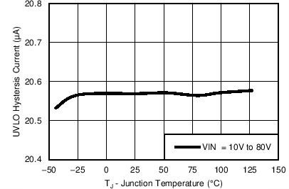
| UVLOHYS | UVLO hysteresis current | UVLO = 1 V | 13 | 20 | 26 | µA |
| UVLOBIAS | UVLO bias current | UVLO = 3 V | 1 | µA | ||
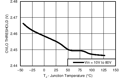
| OVLOTH | OVLO threshold | VOVLO rising | 2.39 | 2.46 | 2.53 | V |
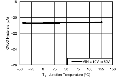
| OVLOHYS | OVLO hysteresis current | OVLO = 1 V | –26 | –21 | –13 | µA |
| OVLOBIAS | OVLO bias current | OVLO = 1 V | 1 | µA | ||
| POWER GOOD (PGD PIN) | ||||||
| PGDVOL | Output low voltage | ISINK = 2 mA | 60 | 110 | mV | |
| PGDIOH | Off leakage current | VPGD = 80 V | 1 | µA | ||
| FB PIN | ||||||
| FBTH | FB threshold | VUVLO = 3 V and VOVLO = 2 V | 2.41 | 2.46 | 2.52 | V |
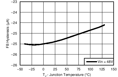
| FBHYS | FB hysteresis current | –25 | –20 | –15 | µA | |
| FBLEAK | Off leakage current | VFB = 2.3 V | 1 | µA | ||
| POWER LIMIT (PWR PIN) | ||||||
| PWRLIM | Power limit sense voltage (VIN-SENSE) | SENSE-OUT = 48 V, RPWR = 121 kΩ | 16.5 | 19.5 | 22.5 | mV |
| SENSE-OUT = 24 V, RPWR = 75 kΩ | 23 | mV | ||||
| IPWR | PWR pin current | VPWR = 2.5 V | –20 | µA | ||
| RSAT(PWR) | PWR pin impedance when disabled | UVLO = 2 V | 135 | Ω | ||
| GATE CONTROL (GATE PIN) | ||||||
| IGATE | Source current | Normal Operation | –26 | –20 | –10 | µA |
| Fault sink current | UVLO = 2 V | 3.4 | 4.2 | 5.3 | mA | |
| POR circuit breaker sink current | VIN – SENSE = 150 mV or VIN < PORIT, VGATE = 5 V | 50 | 115 | 180 | mA | |
| VGATEZ | Reverse-bias voltage of GATE to OUT zener diode | GATE – OUT | 15 | 16.5 | 18 | V |
| VGATECP | Peak charge pump voltage in normal operation (VIN = VOUT) | GATE – OUT | 13.6 | V | ||
| OUT PIN | ||||||
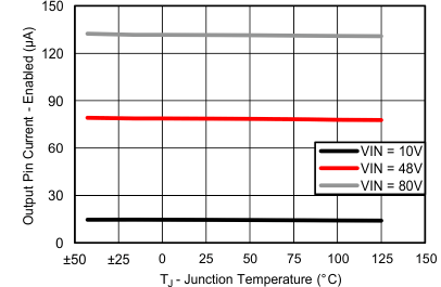
| IOUT-EN | OUT bias current, enabled | OUT = VIN, Normal operation | 78 | µA | ||
| IOUT-DIS | OUT bias current, disabled (2) | Disabled, OUT = 0 V, SENSE = VIN | –50 | µA | ||
| CURRENT LIMIT | ||||||
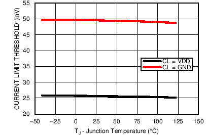
| VCL | Current limit threshold voltage (VIN – VSENSE) |
CL = VDD | 23 | 26 | 29 | mV |
| CL = GND | 47 | 50 | 53 | |||
| ISENSE | SENSE input current | Enabled, SENSE = OUT | 25 | µA | ||
| Disabled, OUT = 0 V | 66 | |||||
| Enabled, OUT = 0 V | 220 | |||||
| CIRCUIT BREAKER | ||||||
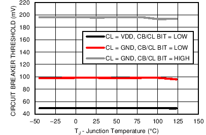
| RTCB | Circuit breaker to current limit ratio: (VIN -VSENSE)CB/VCL | CB/CL ratio bit = 0, ILim = 50 mV | 1.64 | 1.94 | 2.23 | V/V |
| CB/CL ratio bit = 1, ILim = 50 mV | 3.28 | 3.87 | 4.45 | |||
| CB/CL ratio bit = 0, ILim = 26 mV | 1.88 | |||||
| CB/CL ratio bit = 1, ILim = 26 mV | 3.75 | |||||
| VCB | Circuit breaker threshold voltage: (VIN – VSENSE) |
CB/CL ratio bit = 0, ILim = 50 mV | 80 | 96 | 110 | mV |
| CB/CL ratio bit = 1, ILim = 50 mV | 164 | 193 | 222 | |||
| CB/CL ratio bit = 0, ILim = 26 mV | 39 | 48 | 57 | |||
| CB/CL ratio bit = 1, ILim = 26 mV | 79 | 96 | 113 | |||
| TIMER (TIMER PIN) | ||||||
| VTMRH | Upper threshold | 3.74 | 3.9 | 4.07 | V | |
| VTMRL | Lower threshold | Restart cycles | 0.98 | 1.1 | 1.24 | V |
| End of eighth cycle | 0.3 | V | ||||
| Re-enable threshold | 0.3 | V | ||||
| ITIMER | Insertion time current | TIMER pin = 2 V | –5.9 | –4.8 | –3.3 | µA |
| Sink current, end of insertion time | 1.0 | 1.5 | 2.0 | mA | ||
| Fault detection current | –95 | –75 | –50 | µA | ||
| Fault sink current | 1.7 | 2.5 | 3.2 | µA | ||
| DCFAULT | Fault restart duty cycle | 0.5 | % | |||
| INTERNAL REFERENCE | ||||||
| VREF | Reference voltage | 2.93 | 2.97 | 3.02 | V | |
| ADC AND MUX | ||||||
| Resolution | 12 | Bits | ||||
| INL | Integral non-linearity | ADC only | ±4 | LSB | ||
| tACQUIRE | Acquisition + Conversion time | Any channel | 100 | µs | ||
| tRR | Acquisition round robin time | Cycle all channels | 1 | ms | ||
| TELEMETRY ACCURACY | ||||||
| IINFSR | Current input full-scale range | CL = GND | 75.8 | mV | ||
| CL = VDD | 38.2 | mV | ||||
| IINLSB | Current input LSB | CL = GND | 18.5 | µV | ||
| CL = VDD | 9.3 | µV | ||||
| VAUXFSR | VAUX input full-scale range | 2.97 | V | |||
| VAUXLSB | VAUX input LSB | 725 | µV | |||
| VINFSR | Input voltage full-scale range | 89.3 | V | |||
| VINLSB | Input voltage LSB | 21.8 | mV | |||
| IINACC | Input current accuracy | VIN – SENSE = 50 mV, CL = GND | –3.0 | +3.0 | % | |
| VIN – SENSE = 25 mV, CL = VDD | -4.25 | 4.25 | % | |||
| VACC | VAUX, VIN, VOUT | VIN, VOUT = 48 V VAUX = 2.8V |
–2.7 | +2.7 | % | |
| PINACC | Input power accuracy | VIN = 48 V, VIN – SENSE = 50mV, CL = VDD |
–4.5 | +4.5 | % | |
| REMOTE DIODE TEMPERATURE SENSOR | ||||||
| TACC | Temperature accuracy using local diode | TA = 25°C to 85°C | 2 | 10 | °C | |
| Remote diode resolution | 9 | bits | ||||
| IDIODE | External diode current source | High level | 250 | 325 | µA | |
| Low level | 9.4 | µA | ||||
| Diode current ratio | 25.9 | |||||
| PMBus PIN THRESHOLDS (SMBA, SDA, SCL) | ||||||
| VIL | Data, clock input low voltage | 0.9 | V | |||
| VIH | Data, clock input high voltage | 2.1 | 5.5 | V | ||
| VOL | Data output low voltage | ISINK = 3 mA | 0 | 0.4 | V | |
| ILEAK | Input leakage current | SDAI, SMBA,SCL = 5 V | 1 | µA | ||
| CONFIGURATION PIN THRESHOLDS (CL, RETRY) | ||||||
| VIH | Threshold voltage | 3 | V | |||
| ILEAK | Input leakage current | CL, RETRY = 5 V | 5 | µA | ||
(1) Current out of a pin is indicated as a negative value.
(2) OUT bias current (disabled) due to leakage current through an internal 1 MΩ resistance from SENSE to VOUT.
(3) All electrical characteristics having room temperature limits are tested during production at TA = 25°C. All hot and cold limits are specified by correlating the electrical characteristics to process and temperature variations and applying statistical process control.
8.6 SMBus Communications Timing Requirements and Definitions
| PARAMETER | MIN | MAX | UNIT | |
|---|---|---|---|---|
| ƒSMB | SMBus operating frequency | 10 | 400 | kHz |
| tBUF | Bus free time between stop and start condition | 1.3 | µs | |
| tHD:STA | Hold time after (repeated) start condition. After this period, the first clock is generated. | 0.6 | µs | |
| tSU:STA | Repeated start condition setup time | 0.6 | µs | |
| tSU:STO | Stop condition setup time | 0.6 | µs | |
| tHD:DAT | Data hold time | 85 | ns | |
| tSU:DAT | Data setup time | 100 | ns | |
| tTIMEOUT | Clock low time-out(1) | 25 | 35 | ms |
| tLOW | Clock low period | 1.5 | µs | |
| tHIGH | Clock high period(2) | 0.6 | µs | |
| tLOW:SEXT | Cumulative clock low extend time (slave device)(3) | 25 | ms | |
| tLOW:MEXT | Cumulative low extend time (master device)(4) | 10 | ms | |
| tF | Clock or data fall time(5) | 20 | 300 | ns |
| tR | Clock or data rise time(5) | 20 | 300 | ns |
(1) Devices participating in a transfer will timeout when any clock low exceeds the value of tTIMEOUT,MIN of 25 ms. Devices that have detected a timeout condition must reset the communication no later than tTIMEOUT,MAX of 35 ms. The maximum value must be adhered to by both a master and a slave as it incorporates the cumulative stretch limit for both a master (10 ms) and a slave (25 ms).
(2) tHIGH MAX provides a simple method for devices to detect bus idle conditions.
(3) tLOW:SEXT is the cumulative time a slave device is allowed to extend the clock cycles in one message from the initial start to the stop. If a slave exceeds this time, it is expected to release both its clock and data lines and reset itself.
(4) tLOW:MEXT is the cumulative time a master device is allowed to extend its clock cycles within each byte of a message as defined from start-to-ack, ack-to-ack, or ack-to-stop.
(5) Rise and fall time is defined as follows: tR = ( VILMAX – 0.15) to (VIHMIN + 0.15); tF = 0.9 VDD to (VILMAX – 0.15)
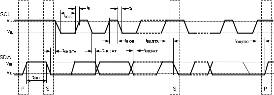 Figure 1. SMBus Timing Diagram
8.7 Switching Characteristics
Unless otherwise stated, the following conditions apply: VVIN = 48 V, –40°C < TJ < 125°C, VUVLO = 3 V , VOVLO = 0 V, RPWR= 20 kΩ.| PARAMETER | CONDITIONS | MIN | TYP | MAX | UNIT | |
|---|---|---|---|---|---|---|
| UVLO/EN, OVLO PINS | ||||||
| UVLODEL | UVLO delay | Delay to GATE high | 9 | µs | ||
| Delay to GATE low | 13 | |||||
| OVLODEL | OVLO delay | Delay to GATE high | 13 | µs | ||
| Delay to GATE low | 10 | |||||
| FB PIN | ||||||
| FBDEL | FB Delay | Delay to PGD high | 7.6 | µs | ||
| Delay to PGD low | 9.2 | |||||
| CURRENT LIMIT | ||||||
| tCL | Response time | VIN-SENSE stepped from 0 to 80 mV; CL = GND | 45 | µs | ||
| CIRCUIT BREAKER | ||||||
| tCB | Response time | VIN-SENSE stepped from 0 to 150 mV, time to GATE low, no load | 0.42 | 0.83 | µs | |
| TIMER (TIMER PIN) | ||||||
| tFAULT_DELAY | Fault to GATE low delay | TIMER pin reaches the upper threshold | 12 | µs | ||
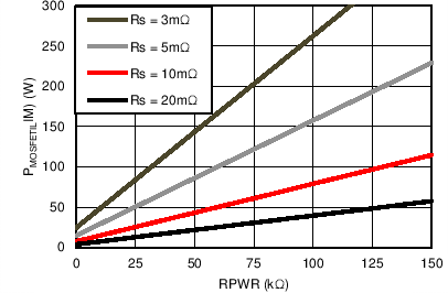
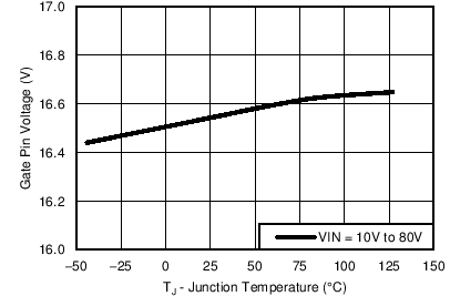
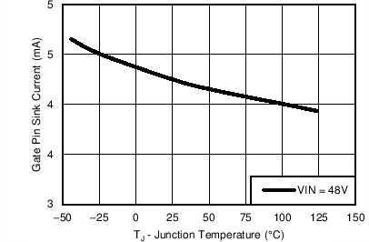
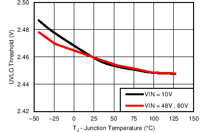
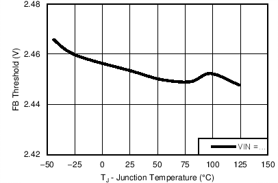
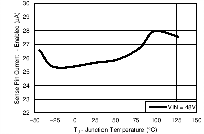
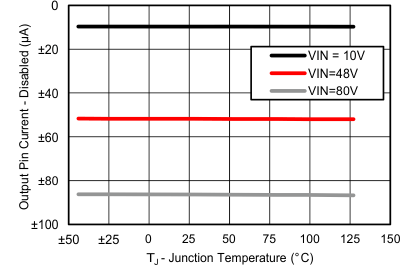
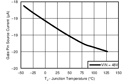
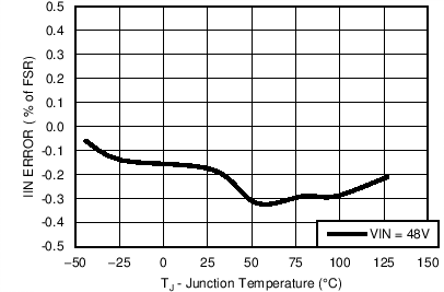
8.8 Typical Performance Characteristics
Unless otherwise specified the following conditions apply: TJ = 25°C, VIN = 48 V. All graphs show junction temperature.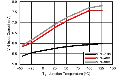
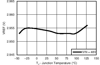
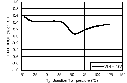
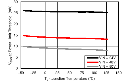
(VIN – Sense = 50 mV)