ZHCSL85B May 2020 – April 2021 AMC3306M25
PRODUCTION DATA
- 1 特性
- 2 應用
- 3 說明
- 4 Revision History
- 5 Pin Configuration and Functions
-
6 Specifications
- 6.1 Absolute Maximum Ratings
- 6.2 ESD Ratings
- 6.3 Recommended Operating Conditions
- 6.4 Thermal Information
- 6.5 Power Ratings
- 6.6 Insulation Specifications
- 6.7 Safety-Related Certifications
- 6.8 Safety Limiting Values
- 6.9 Electrical Characteristics
- 6.10 Switching Characteristics
- 6.11 Timing Diagrams
- 6.12 Insulation Characteristics Curves
- 6.13 Typical Characteristics
- 7 Detailed Description
- 8 Application and Implementation
- 9 Power Supply Recommendations
- 10Layout
- 11Device and Documentation Support
- 12Mechanical, Packaging, and Orderable Information
5 Pin Configuration and Functions
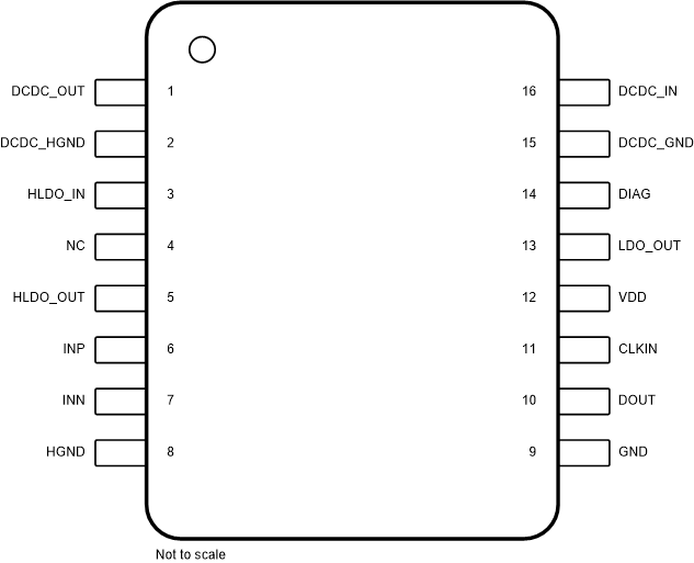
 Figure 5-1 DWE Package,16-Pin SOIC,Top View
Table 5-1 Pin Functions
| PIN | TYPE | DESCRIPTION | |
|---|---|---|---|
| NO. | NAME | ||
| 1 | DCDC_OUT | Power | High-side output of the DC/DC converter; connect this pin to the HLDO_IN pin.(1) |
| 2 | DCDC_HGND | High-side Power Ground | High-side ground reference for the DC/DC converter; connect this pin to the HGND pin. |
| 3 | HLDO_IN | Power | Input of the high-side LDO; connect this pin to the DCDC_OUT pin.(1) |
| 4 | NC | — | No internal connection. Connect this pin to the high-side ground or leave unconnected (floating). |
| 5 | HLDO_OUT | Power | Output of the high-side LDO.(1) |
| 6 | INP | Analog Input | Noninverting analog input. Either INP or INN must have a DC current path to HGND to define the common-mode input voltage.(2) |
| 7 | INN | Analog Input | Inverting analog input. Either INP or INN must have a DC current path to HGND to define the common-mode input voltage.(2) |
| 8 | HGND | High-side Signal Ground | High-side analog signal ground; connect this pin to the DCDC_HGND pin. |
| 9 | GND | Low-side Signal Ground | Low-side analog signal ground; connect this pin to the DCDC_GND pin. |
| 10 | DOUT | Digital Output | Modulator data output. |
| 11 | CLKIN | Digital Input | Modulator clock input with internal pulldown resistor (typical value: 1.5 MΩ). |
| 12 | VDD | Low-side Power | Low-side power supply.(1) |
| 13 | LDO_OUT | Power | Output of the low-side LDO; connect this pin to the DCDC_IN pin. The output of the LDO must not be loaded by external circuitry.(1) |
| 14 | DIAG | Digital Output | Active-low, open-drain status indicator output; connect this pin to the pullup supply (for example, VDD) using a resistor or leave this pin floating if not used. |
| 15 | DCDC_GND | Low-side Power Ground | Low-side ground reference for the DC/DC converter; connect this pin to the GND pin. |
| 16 | DCDC_IN | Power | Low-side input of the DC/DC converter; connect this pin to the LDO_OUT pin.(1) |
(1) See the Section 9 section for power-supply decoupling
recommendations.
(2) See the Section 10 section for details.