ZHCSI83C may 2018 – may 2023 ADC12DL3200
PRODUCTION DATA
- 1
- 1特性
- 2應(yīng)用
- 3說(shuō)明
- 4Revision History
- 5Pin Configuration and Functions
-
6Specifications
- 6.1 Absolute Maximum Ratings
- 6.2 ESD Ratings
- 6.3 Recommended Operating Conditions
- 6.4 Thermal Information
- 6.5 Electrical Characteristics: DC Specifications
- 6.6 Electrical Characteristics: Power Consumption
- 6.7 Electrical Characteristics: AC Specifications (Dual-Channel Mode)
- 6.8 Electrical Characteristics: AC Specifications (Single-Channel Mode)
- 6.9 Timing Requirements
- 6.10 Switching Characteristics
- 6.11 Typical Characteristics
-
7Detailed Description
- 7.1 Overview
- 7.2 Functional Block Diagram
- 7.3
Feature Description
- 7.3.1 Analog Inputs
- 7.3.2 ADC Core
- 7.3.3 Timestamp
- 7.3.4 Clocking
- 7.3.5 LVDS Digital Interface
- 7.3.6 Alarm Monitoring
- 7.3.7 Temperature Monitoring Diode
- 7.3.8 Analog Reference Voltage
- 7.4
Device Functional Modes
- 7.4.1 Dual-Channel Mode (Non-DES Mode)
- 7.4.2 Internal Dither Modes
- 7.4.3 Single-Channel Mode (DES Mode)
- 7.4.4 LVDS Output Driver Modes
- 7.4.5 LVDS Output Modes
- 7.4.6 Power-Down Modes
- 7.4.7 Calibration Modes and Trimming
- 7.4.8 Offset Calibration
- 7.4.9 Trimming
- 7.5 Programming
- 7.6 Register Maps
- Application and Implementation
- 8Device and Documentation Support
- 9Mechanical, Packaging, and Orderable Information
封裝選項(xiàng)
機(jī)械數(shù)據(jù) (封裝 | 引腳)
散熱焊盤(pán)機(jī)械數(shù)據(jù) (封裝 | 引腳)
訂購(gòu)信息
8.5.2 Layout Example
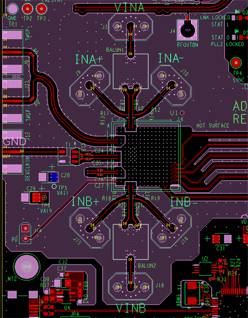
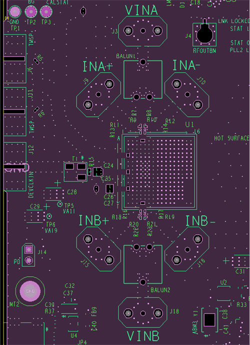
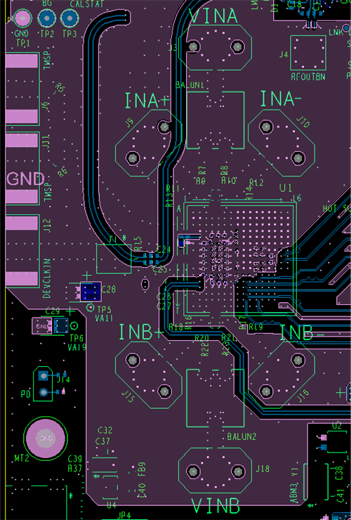
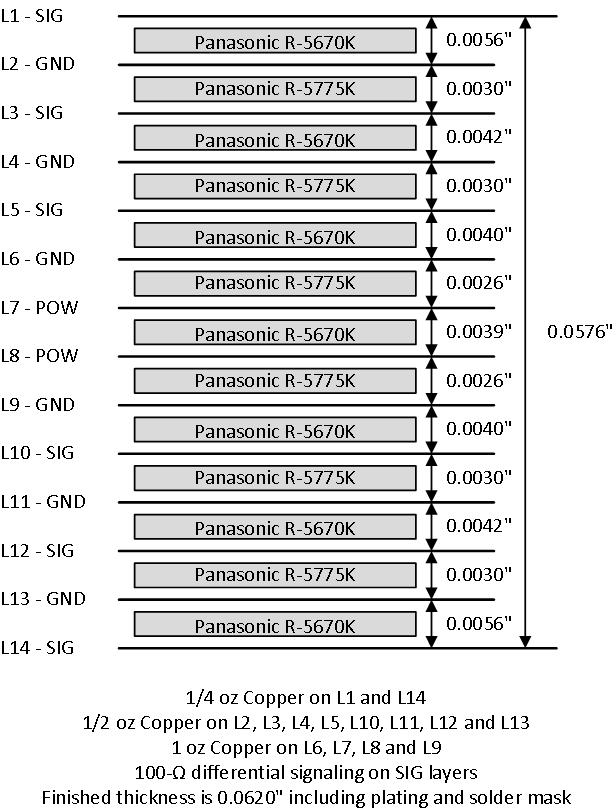
Figure 8-14 to Figure 8-16 provide examples of the critical traces routed on the device evaluation module (EVM). Figure 8-17 provides an example printed circuit board (PCB) layer stackup.
 Figure 8-14 Top Layer Routing: Analog Inputs, CLK and SYSREF, DA0-3, DB0-3
 Figure 8-15 GND1 Cutouts to Optimize Impedance of Component Pads
 Figure 8-16 Bottom Layer Routing: Additional CLK Routing, DA4-7, DB4-7
 Figure 8-17 Example PCB Stackup