SNVU794 September 2021 LM61430-Q1
4 Board Layout
The PCB consists of a 4-layer design. There are 2-oz copper planes on the top and bottom and 1-oz copper mid-layer planes to dissipate heat with an array of thermal vias to connect to all four layers.
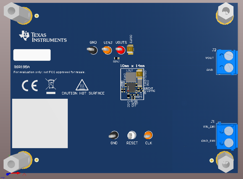 Figure 4-1 Top 3-D View
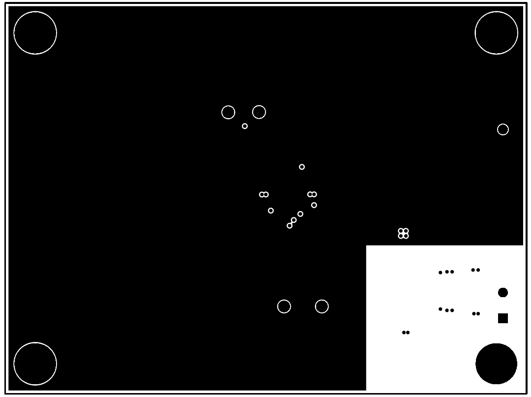 Figure 4-3 Signal Layer 1 – Ground
Plane
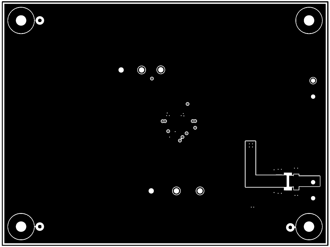 Figure 4-5 Bottom Layer
 Figure 4-2 Top Layer
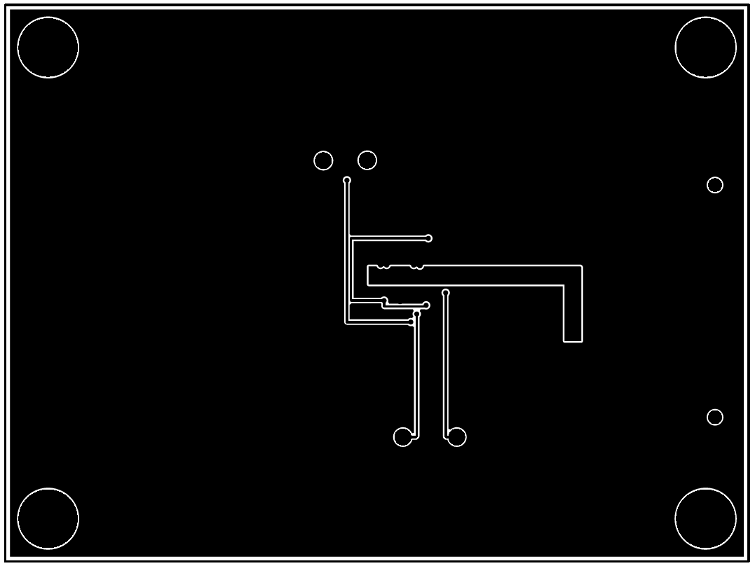 Figure 4-4 Signal Layer 2 –
Routing
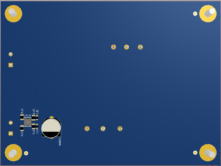 Figure 4-6 Bottom 3-D View