SNVA919A January 2020 – July 2020 LM25180 , LM25180-Q1 , LM5180 , LM5180-Q1 , LM5181 , LM5181-Q1
4 Pin Failure Mode Analysis (Pin FMA)
This section provides a Failure Mode Analysis (FMA) for the pins of the LM5180, LM5180-Q1, LM25180, LM25180-Q1, LM5181, and LM5181-Q1. The failure modes covered in this document include the typical pin-by-pin failure scenarios:
- Pin short-circuited to Ground (see Table 4-2)
- Pin open-circuited (see Table 4-3)
- Pin short-circuited to an adjacent pin (see Table 4-4)
- Pin short-circuited to supply (see Table 4-5)
Table 4-2 through Table 4-5 also indicate how these pin conditions can affect the device as per the failure effects classification in Table 4-1.
| Class | Failure Effects |
|---|---|
| A | Potential device damage that affects functionality |
| B | No device damage, but loss of functionality |
| C | No device damage, but performance degradation |
| D | No device damage, no impact to functionality or performance |
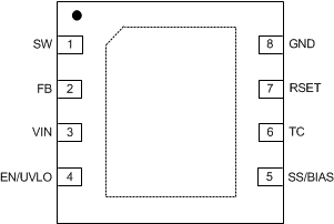
Figure 4-1 shows the LM5180, LM5180-Q1, LM25180, LM25180-Q1, LM5181, and LM5181-Q1 pin diagram. For a detailed description of the device pins please refer to the Pin Configuration and Functions section in the LM5180, LM5180-Q1, LM25180, LM25180-Q1, LM5181, and LM5181-Q1 data sheets.
 Figure 4-1 Pin Diagram
| Pin Name | Pin No. | Description of Potential Failure Effect(s) | Failure Effect Class |
|---|---|---|---|
| SW | 1 | VOUT = 0 V; Damage to transformer | A |
| FB | 2 | VOUT = 0 V; Damage VIN to FB | A |
| VIN | 3 | VOUT = 0 V | B |
| EN/UVLO | 4 | VOUT = 0 V; Shutdown operation | B |
| SS/BIAS | 5 | VOUT = 0 V if short during start-up. VOUT normal if short during steady-state | B |
| TC | 6 | Temperature compensation disabled; VOUT target will be slightly different due to Rtc||Rset | C |
| RSET | 7 | VOUT = ISW-PEAK*tOFF*Rload*NPS/240 μs; 120 μs switching | B |
| GND | 8 | Normal operation. | D |
| Pin Name | Pin No. | Description of Potential Failure Effect(s) | Failure Effect Class |
|---|---|---|---|
| SW | 1 | VOUT = 0 V; No switching | B |
| FB | 2 | VOUT = 0 V; 120 μs switching | B |
| VIN | 3 | VOUT = 0 V | B |
| EN/UVLO | 4 | Shutdown or Regulating since EN is high impedance | B |
| SS/BIAS | 5 | VOUT regulating; Internal SS only | C |
| TC | 6 | VOUT regulating; Temperature compensation disabled | C |
| RSET | 7 | VOUT = 0 V; VOUT cannot be sensed | B |
| GND | 8 | Floating GND | B |
| Pin Name | Pin No. | Description of Potential Failure Effect(s) | Failure Effect Class |
|---|---|---|---|
| SW | 1 | VOUT = 0 V; Damage VIN to FB diode | A |
| FB | 2 | VOUT = 0 V; VOUT cannot be sensed | B |
| VIN | 3 | VOUT regulating; Always in ACTIVE mode | C |
| EN/UVLO | 4 | -- | -- |
| SS/BIAS | 5 | Current limit threshold will be lower | B |
| TC | 6 | VOUT = ISW-PEAK*tOFF*Rload*NPS/240 μs depending on TC; VOUT cannot be sensed | B |
| RSET | 7 | VOUT = ISW-PEAK*tOFF*Rload*NPS/240 μs depending on TC; VOUT cannot be sensed | B |
| GND | 8 | -- |
| Pin Name | Pin No. | Description of Potential Failure Effect(s) | Failure Effect Class |
|---|---|---|---|
| SW | 1 | VOUT = 0 V; Damage SW to GND | A |
| FB | 2 | VOUT = 0 V; VOUT cannot be sensed | B |
| VIN | 3 | Normal Operation | D |
| EN/UVLO | 4 | VOUT regulating; Always in ACTIVE mode | C |
| SS/BIAS | 5 | Damage to 15 V ESD on SS/BIAS | A |
| TC | 6 | Damage to 5 V ESD on TC | A |
| RSET | 7 | Damage to 5 V ESD on RSET | A |
| GND | 8 | VOUT = 0 V | B |