SLUP412 February 2022 LMG3522R030-Q1
- 1 Introduction
- 2 Comparing Different Technologies
- 3 Advantages of Integrating the Driver With GaN FETs
- 4 The GaN-Based 6.6-kW OBC Reference Design
- 5 PFC Stage
- 6 DC/DC Stage
- 7 DC/DC Topology Selection
- 8 Frequency Selection
- 9 Core Loss
- 10Loss of ZVS
- 11Dead Time
- 12ISR Bandwidth
- 13Overall
- 14Resonant Tank Design
- 15Thermal Solution
- 16Layout Best Practices
- 17Control-Loop Considerations
- 18Conclusions
- 19References
- 20Important Notice
15 Thermal Solution
Figure 15-1 shows the complete solution with the cold plate attached. The solution uses liquid cooling with a maximum coolant temperature of 65°C. All hot components access the cold plate from the back side of the printed wiring board (PWB).
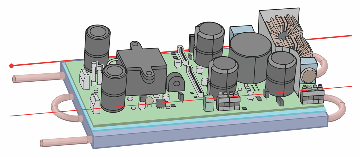 Figure 15-1 3D image of the complete
solution.
Figure 15-1 3D image of the complete
solution.Figure 15-2 shows a cross-section of this solution illustrating how the GaN FETs interface to the PWB and cold plate. Using a thermal interface material (TIM) will facilitate heat transfer from all hot spots.
Figure 15-2 also shows the placement of the TIM relative to the cold plate and GaN FETs. The FETs themselves have a θJunction-Case of 0.15°C/W. The TIM has a thermal impedance of 1.2 to 1.25°C/W. Overall, θJunction-ColdPlate is 1.35 to 1.5°C/W.
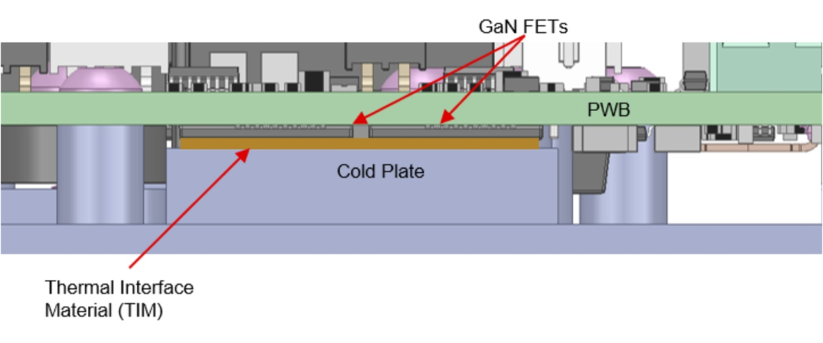 Figure 15-2 Magnified cross-section of the
6.6-kW OBC reference design PWB.
Figure 15-2 Magnified cross-section of the
6.6-kW OBC reference design PWB.Figure 15-3 shows the bottom side of the PWB, while Figure 15-4 shows the top side of the cold plate. By comparing these images, you can see how the cold-plate features provide access to the thermally significant components highlighted in Figure 15-3.
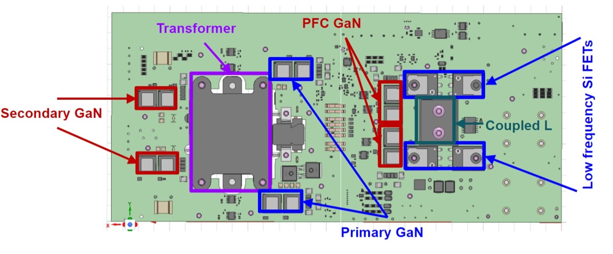 Figure 15-3 Bottom view of the 6.6-kW OBC
reference design PWB.
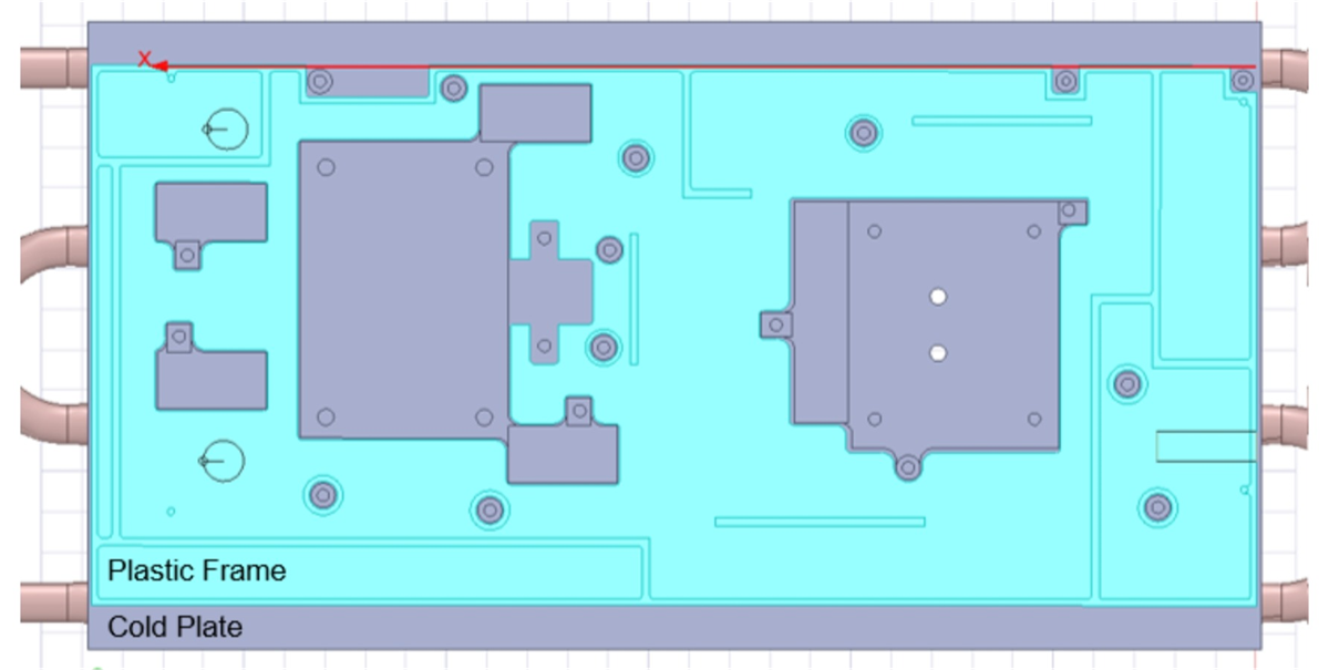 Figure 15-4 Top view of the liquid-cooled
cold plate.
Figure 15-4 Top view of the liquid-cooled
cold plate.Figure 15-5 is a thermal scan of the top side of the board. Given that the significantly hot components are located on the bottom side, there is very little of interest to see here.
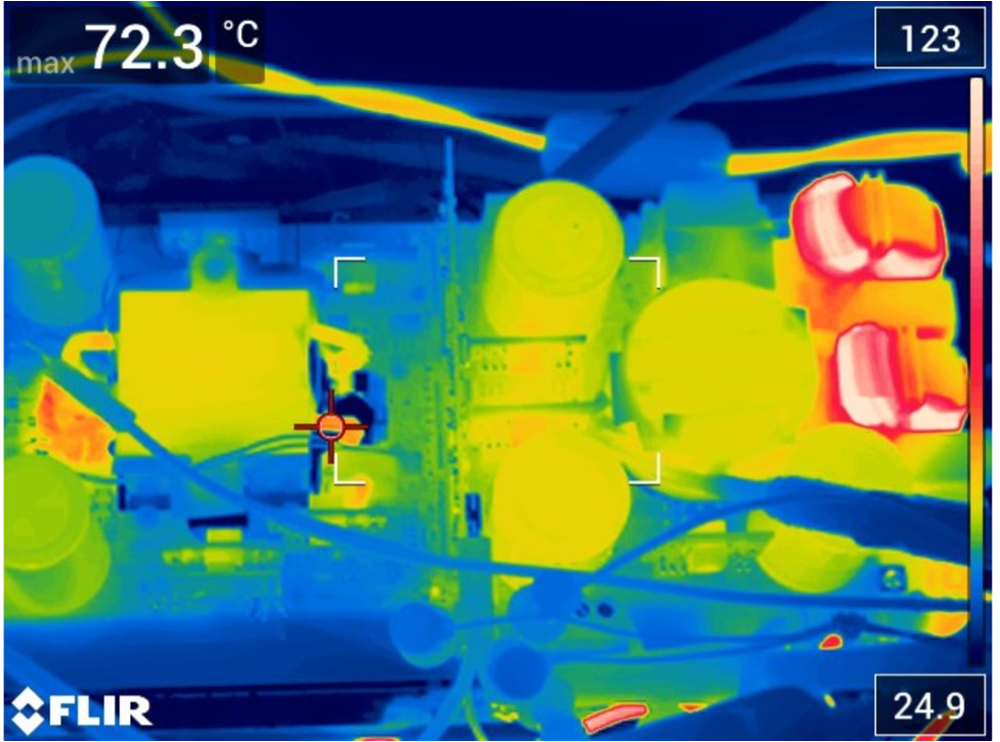 Figure 15-5 Thermal scan of the top side
of the 6.6-kW OBC.