SLLA590 May 2022 THVD8000 , THVD8010
- Abstract
- Trademarks
- 1Introduction
-
2THVD80x0 Devices Theory of Operation and
Limitations of Use
- 2.1 Overview and Similarities between Standard RS-485 Transceivers and THVD80xo Devices
- 2.2 Differences between Standard RS-485 Transceivers and THVD8000/8010
- 2.3 Standard Approach to Using THVD80xo Devices to Communicate over Power Lines
- 2.4 Drawbacks to Standard Approach with Higher Voltage Systems
- 3Integration of Line Driver with THVD80x0 Devices to Drive Low Impedance Loads
- 4High Voltage Interface and Communication Interface Power Supply
- 5System Level View and Relation to Higher Voltage Implementations
- 6Summary
- 7References
5.2 System Overview with Selected Test Results
With the system fully explained it is time to look at how all these parts mesh together as well as look at some test data from a couple different implementations of these designs. Figure 5-1, Figure 5-2, Figure 5-3, and Figure 5-4 show the schematics of the THVD8000 (TX/RX), line driver interface, protection/filtering/high voltage interface, and the power tree respectively.
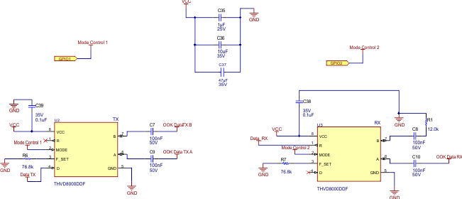 Figure 5-1 THVD8000 Schematic
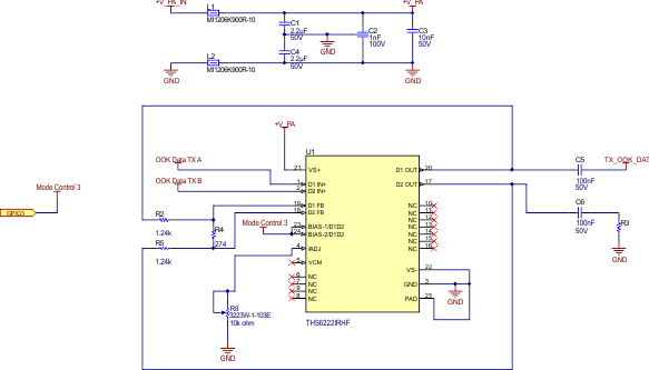 Figure 5-2 THS6222 Schematic
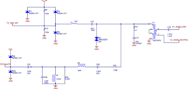 Figure 5-3 Protection/Bandpass/HV Interface Schematic
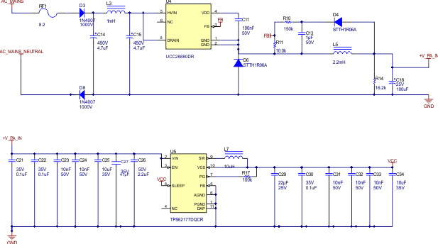 Figure 5-4 Power Tree Schematic
| Component PN# | Comment |
|---|---|
| 750510476 | Werth Elektronik transformer |
| C4AQSBU4150A1XJ | 1.5uF | 1.5kV Capacitor KEMET |
This application uses a data rate of 2KHz, 110VAC line, modulation frequency of 125 KHz, a 16 V power supply for the THS6222 (±8 V), and a 3.3 V power supply for MCU and THVD8000. Test results are shown in Figure 5-5 through Figure 5-9 where TX and RX are the input/output of the THVD8000 respectively.
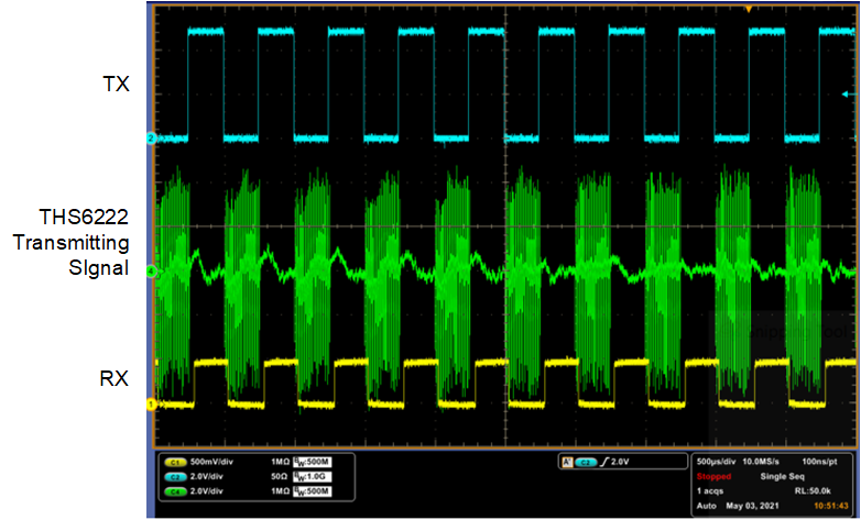 Figure 5-5 THVD8000 RX and TX signals; THS6222 Transmitting Signals
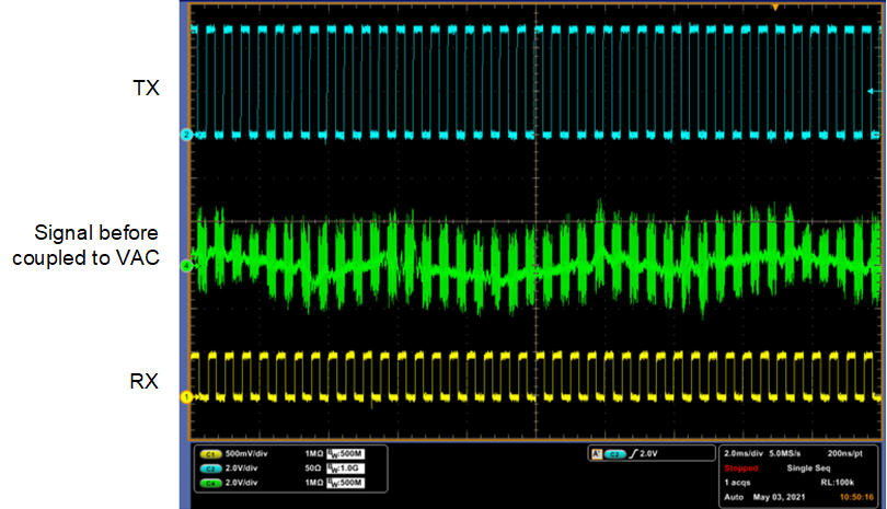 Figure 5-6 THVD8000 RX and TX signals; THS6222 Transmitting Signals - Zoomed Out
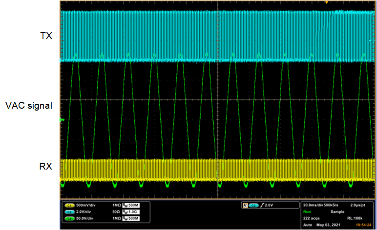 Figure 5-7 TX/RX data Overlaid on VAC Signal
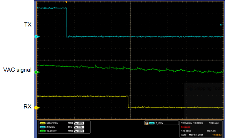 Figure 5-8 TX/RX data Overlaid on VAC Signal Zoomed In
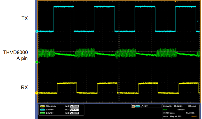 Figure 5-9 THVD8000 RX Signal on "A" Pin