ZHCSFN1A November 2016 – January 2022 UCC20520
PRODUCTION DATA
- 1 特性
- 2 應(yīng)用
- 3 說明
- 4 Revision History
- 5 Pin Configuration and Functions
-
6 Specifications
- 6.1 Absolute Maximum Ratings
- 6.2 ESD Ratings
- 6.3 Recommended Operating Conditions
- 6.4 Thermal Information
- 6.5 Power Ratings
- 6.6 Insulation Specifications
- 6.7 Safety-Related Certifications
- 6.8 Safety-Limiting Values
- 6.9 Electrical Characteristics
- 6.10 Switching Characteristics
- 6.11 Insulation Characteristics Curves
- 6.12 Typical Characteristics
- 7 Parameter Measurement Information
- 8 Detailed Description
-
9 Application and Implementation
- 9.1 Application Information
- 9.2
Typical Application
- 9.2.1 Design Requirements
- 9.2.2
Detailed Design Procedure
- 9.2.2.1 Designing PWM Input Filter
- 9.2.2.2 Select External Bootstrap Diode and its Series Resistor
- 9.2.2.3 Gate Driver Output Resistor
- 9.2.2.4 Estimate Gate Driver Power Loss
- 9.2.2.5 Estimating Junction Temperature
- 9.2.2.6 Selecting VCCI, VDDA/B Capacitor
- 9.2.2.7 Dead Time Setting Guidelines
- 9.2.2.8 Application Circuits with Output Stage Negative Bias
- 9.2.2.9 56
- 9.2.3 Application Curves
- 10Layout
- 11Device and Documentation Support
封裝選項
機械數(shù)據(jù) (封裝 | 引腳)
- DW|16
散熱焊盤機械數(shù)據(jù) (封裝 | 引腳)
- DW|16
訂購信息
6.12 Typical Characteristics
VDDA = VDDB= 12 V, VCCI = 3.3 V, TA = 25°C, No load unless otherwise noted.

| No load |

| CLOAD = 10 nF |
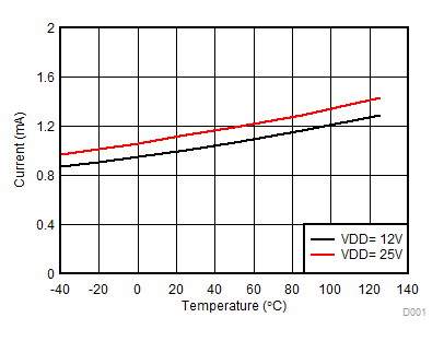
| No load | Input low | No switching |
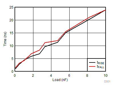
| VDD = 12 V |
 Figure 6-12 Propagation Delay vs. Temperature
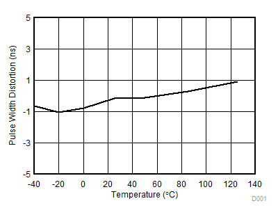 Figure 6-14 Pulse Width Distortion vs. Temperature
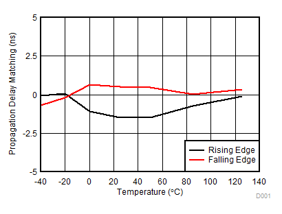 Figure 6-16 Propagation Delay Matching (tDM) vs. Temperature
 Figure 6-18 VDD UVLO Threshold vs. Temperature
 Figure 6-20 PWM/DIS Low Threshold
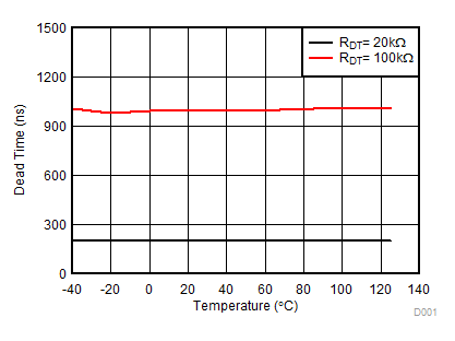 Figure 6-22 Dead Time vs.
Temperature
 Figure 6-24 Typical Output
Voltage
| CLOAD = 1 nF |
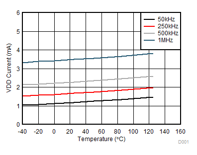
| No load |
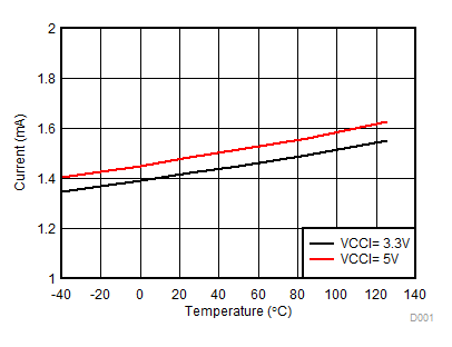
| No load | DIS is high | No switching |
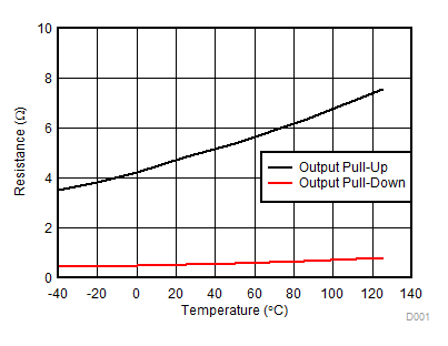 Figure 6-11 Output Resistance vs. Temperature
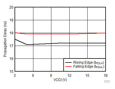 Figure 6-13 Propagation Delay vs. VCCI
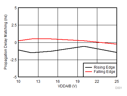 Figure 6-15 Propagation Delay Matching (tDM) vs. VDD
 Figure 6-17 VDD UVLO Hysteresis vs. Temperature
 Figure 6-19 PWM/DIS Hysteresis vs. Temperature
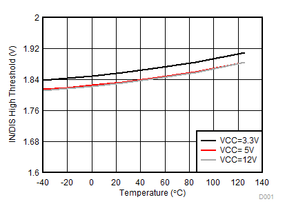 Figure 6-21 PWM/DIS High Threshold
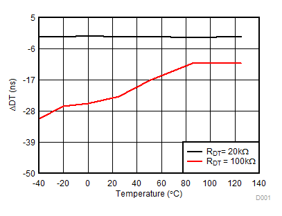 Figure 6-23 Dead Time Matching vs.
Temperature