ZHCSGQ4 September 2017 TUSB213-Q1
PRODUCTION DATA.
- 1 特性
- 2 應(yīng)用
- 3 說(shuō)明
- 4 修訂歷史記錄
- 5 Pin Configuration and Functions
- 6 Specifications
- 7 Detailed Description
- 8 Application and Implementation
- 9 Power Supply Recommendations
- 10Layout
- 11器件和文檔支持
- 12機(jī)械、封裝和可訂購(gòu)信息
封裝選項(xiàng)
請(qǐng)參考 PDF 數(shù)據(jù)表獲取器件具體的封裝圖。
機(jī)械數(shù)據(jù) (封裝 | 引腳)
- RGY|14
散熱焊盤(pán)機(jī)械數(shù)據(jù) (封裝 | 引腳)
訂購(gòu)信息
6 Specifications
6.1 Absolute Maximum Ratings
over operating free-air temperature and voltage range (unless otherwise noted)(1)| MIN | MAX | UNIT | ||
|---|---|---|---|---|
| Supply Voltage Range | VCC | -0.3 | 6 | V |
| Voltage Range on I/O pins | DxP, DxM, RSTN, EQ, SCL, SDA, DC_BOOST, VREG | -0.3 | 3.8 | V |
| Tstg | Storage temperature | -65 | 150 | °C |
(1) Stresses beyond those listed under Absolute Maximum Rating may cause permanent damage to the device. These are stress ratings only, which do not imply functional operation of the device at these or any other conditions beyond those indicated under Recommended Operating Condition. Exposure to absolute-maximum-rated conditions for extended periods may affect device reliability.
6.2 ESD Ratings
| VALUE | UNIT | |||
|---|---|---|---|---|
| V(ESD) | Electrostatic discharge | Human body model (HBM), per ANSI/ESDA/JEDEC JS-001, all pins(1) | ±2000 | V |
| Charged device model (CDM), per JEDEC specification JESD22-C101, all pins(2) | ±500 | |||
(1) JEDEC document JEP155 states that 500-V HBM allows safe manufacturing with a standard ESD control process.
(2) JEDEC document JEP157 states that 250-V CDM allows safe manufacturing with a standard ESD control process.
6.3 Recommended Operating Conditions
over operating free-air temperature and voltage range (unless otherwise noted)| MIN | NOM | MAX | UNIT | |||
|---|---|---|---|---|---|---|
| VCC | Supply voltage | 4.4 | 5 | 5.5 | V | |
| TA | Ambient temperature | TUSB213Q1 | -40 | 105 | °C | |
| TJ | Junction temperature | TUSB213Q1 | -40 | 125 | °C | |
6.4 Thermal Information
| THERMAL METRIC(1) | UNIT | ||
|---|---|---|---|
| RGY (VQFN) | |||
| 14 PINS | |||
| RθJA | Junction-to-ambient thermal resistance | 49.1 | °C/W |
| RθJC(top) | Junction-to-case (top) thermal resistance | 52.8 | °C/W |
| RθJB | Junction-to-board thermal resistance | 24.2 | °C/W |
| ΨJT | Junction-to-top characterization parameter | 2.2 | °C/W |
| ΨJB | Junction-to-board characterization parameter | 24.3 | °C/W |
| RθJC(bot) | Junction-to-case (bottom) thermal resistance | 7 | °C/W |
(1) For more information about traditional and new thermal metrics, see the Semiconductor and IC Package Thermal Metrics application report.
6.5 Electrical Characteristics
over operating free-air temperature and voltage range (unless otherwise noted)| PARAMETER | TEST CONDITIONS | MIN | TYP | MAX | UNIT | |
|---|---|---|---|---|---|---|
| POWER | ||||||
| IACTIVE_HS | High-speed active curent | USB channel = HS mode; 480 Mbps traffic; VCC = 5V; VCC supply stable; DC Boost = 60 mV | 18 | 30 | mA | |
| IIDLE_HS | High-speed idle current | USB channel = HS mode; no traffic; VCC = 5V; VCC supply stable; DC Boost = 60 mV | 13 | 22 | mA | |
| ISUSPEND_HS | High-speed suspend current | USB channel = HS suspend mode; VCC = 5V; VCC supply stable | 0.76 | 1.5 | mA | |
| IFS_LS | Full/Low speed current | USB channel = FS mode or LS mode; VCC = 5V | 0.77 | 1.5 | mA | |
| IDISCONNECT | Disconnect current | Host side application; No device attachment; VCC = 5V | 0.86 | 1.5 | mA | |
| IRSTN | Disable current | RSTN driven low; VCC supply stable; VCC = 5V | 22 | 80 | µA | |
| ILKG_FS | Pin fail-safe leakage current for SDA, SCL, DC_BOOST, DxP/N, RSTN | VCC = 0 V; Pin at 3.6 V | 40 | µA | ||
| RSTN | ||||||
| VIH | High-level input voltage | VCC = 4.4V | 2 | 3.6 | V | |
| VIL | Low-level input voltage | VCC = 5.5V | 0 | 0.8 | V | |
| IIH | High-level input current | VIH = 3.6 V | -4 | 4 | µA | |
| IIL | Low-level input current | VIL = 0 V | -11 | 11 | µA | |
| EQ | ||||||
| REQ | External pull-down resistor on EQ pin. | AC Boost Level 0 | 160 | Ω | ||
| AC Boost Level 1 | 1.4 | 2 | kΩ | |||
| AC Boost Level 2 | 3.7 | 3.9 | kΩ | |||
| AC Boost Level 3 | 6 | kΩ | ||||
| CD, ENA_HS | ||||||
| VOH | High-level output voltage | IO = -50µA | 2.4 | V | ||
| VOL | Low-level output voltage | IO = 50µA | 0.4 | V | ||
| SCL, SDA | ||||||
| CI2CBUS | I2C Bus capacitance | 4 | 150 | pF | ||
| VIH | SDA and SCL input high level voltage | VCC = 4.4V | 2 | 3.6 | V | |
| VIL | SDA and SCL input Low level voltage | VCC = 5.5V | 0.8 | V | ||
| VSDA_OL | SDA low-level output voltage | 4.7kΩ pullup to 3.6V; VCC = 4.4V | 0.4 | V | ||
| ISDA_OL | SDA Low level output current | VCC = 5.5V; I2C pulled up to 3.6V | 1.1 | mA | ||
| DC_BOOST | ||||||
| VIH | High-level input voltage | VCC = 5V | 2.4 | 3.6 | V | |
| VIM | Mid-level input voltage | VCC = 5V | 1.6 | V | ||
| VIL | Low-level input voltage | VCC = 5V | 0 | 0.4 | V | |
| DxP, DxM | ||||||
| CIO_DXX | Capacitance to GND | Measured with LCR meter and device powered down. 1 MHz sinusoid, 30 mVpp ripple | 2.7 | pF | ||
6.6 Switching Characteristics
over operating free-air temperature and voltage range (unless otherwise noted)| PARAMETER | TEST CONDITIONS | MIN | TYP | MAX | UNIT | |
|---|---|---|---|---|---|---|
| FBR_DXX | DxP/M Bit Rate | USB channel = HS mode; 480 Mbps traffic; VCC supply stable | 480.24 | Mbps | ||
| tRISE_DXX | DxP/M rise time | 10% - 90%; VCC = 5.5V; Max AC Gain; | 100 | ps | ||
| tFALL_DXX | DxP/M fall time | 90% - 10%; VCC = 5.5V; Max AC Gain; | 100 | ps | ||
| tRSTN_PULSE_WIDTH | Minimum width to detect a valid RSTN signal assert when the pin is actively driven | VCC = 4.4 V; Refer to Figure 1 | 20 | µs | ||
| tSTABLE | VCC stable before RSTN de-assertion | Refer to Figure 1 | 100 | µs | ||
| tVCC_RAMP | VCC ramp time | 0.2 | 100 | ms | ||
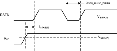 Figure 1. Power On and Reset Timing
6.7 Typical Characteristics
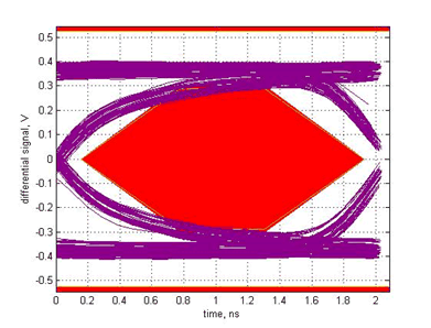 Figure 2. USB2.0 HS Eye diagram, Host far-end with 2m cable post-channel loss without TUSB213-Q1
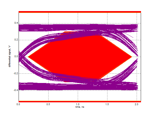 Figure 4. USB2.0 HS Eye diagram, Host far-end with 5m cable pre-channel loss without TUSB213-Q1
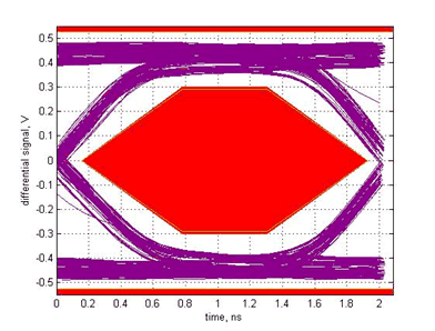 Figure 3. USB2.0 HS Eye diagram, Host far-end with 2m cable post-channel loss with TUSB213-Q1
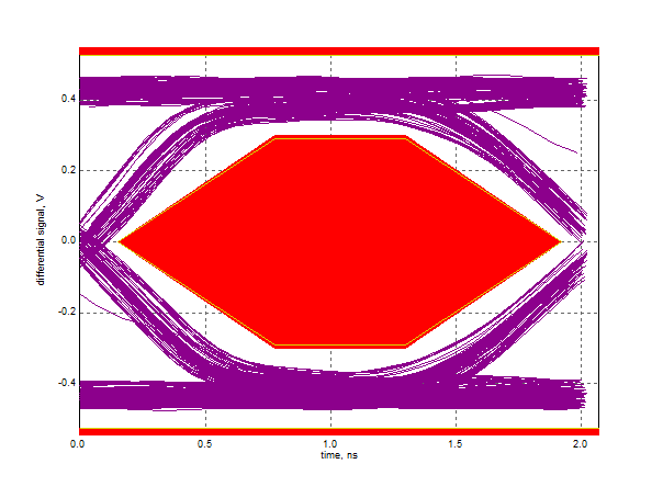 Figure 5. USB2.0 HS Eye diagram, Host far-end with 5m cable pre-channel loss with TUSB213-Q1