ZHCSCS9 SEPTEMBER 2014 TPS92661-Q1
PRODUCTION DATA.
- 1 特性
- 2 應(yīng)用
- 3 說明
- 4 修訂歷史記錄
- 5 Pin Configuration and Functions
- 6 Specifications
-
7 Detailed Description
- 7.1 Overview
- 7.2 Functional Block Diagram
- 7.3
Feature Description
- 7.3.1 Controlling the Internal LED Bypass Switches
- 7.3.2 Internal Switch Resistance
- 7.3.3 PWM Dimming
- 7.3.4 PWM Clock
- 7.3.5 PWM Synchronization
- 7.3.6 Switch Slew Control
- 7.3.7 Effect of Phase Shifting LED Duty Cycles
- 7.3.8 LED Fault Detection and Protection
- 7.3.9 Glitch-Free Operation
- 7.3.10 Internal Oscillator and Watchdog Timers
- 7.4
Device Functional Modes
- 7.4.1
Digital Interface Connections
- 7.4.1.1 Address (ADR0, ADR1, and ADR2 Pins)
- 7.4.1.2 Clock (CLK Pin)
- 7.4.1.3 Internal Charge Pump (CPP Pin)
- 7.4.1.4 Enable (EN Pin)
- 7.4.1.5 GND Pin
- 7.4.1.6 Receive (RX Pin)
- 7.4.1.7 Synchronization (SYNC Pin)
- 7.4.1.8 Transmit (TX Pin)
- 7.4.1.9 Primary Power Supply (VIN Pin)
- 7.4.1.10 On-Board 3.3-V Supply (VCC Pin)
- 7.4.2 Internal Pin-to-Pin Resistance
- 7.4.3 UART Physical Layer
- 7.4.4 UART Clock and Baudrate
- 7.4.5 UART Communications Reset
- 7.4.6 UART Device Addressing
- 7.4.7 UART Communications Protocol
- 7.4.8 Transaction Frame Description
- 7.4.9 Frame Initialization Byte
- 7.4.10 Register Address
- 7.4.11 Data Bytes
- 7.4.12 CRC Bytes
- 7.4.13 Registers
- 7.4.1
Digital Interface Connections
- 7.5 Programming
- 7.6 Register Map
- 8 Application and Implementation
- 9 Power Supply Recommendations
- 10Layout
- 11器件和文檔支持
- 12機(jī)械封裝和可訂購信息
封裝選項(xiàng)
機(jī)械數(shù)據(jù) (封裝 | 引腳)
- PHP|48
散熱焊盤機(jī)械數(shù)據(jù) (封裝 | 引腳)
- PHP|48
訂購信息
6 Specifications
6.1 Absolute Maximum Ratings(1)(2)
Over operating free-air temperature range (unless otherwise noted)| MIN | MAX | UNIT | ||
|---|---|---|---|---|
| Input voltage | VIN, VCC to GND | –0.3 | 7 | V |
| CPP to GND | –0.3 | 67 | ||
| CPP to LED12 | –0.3 | 7 | ||
| LEDx to GND | –0.3 | 60 | ||
| LEDx to LED(x-1) | –0.3 | 7 | ||
| SYNC, EN, CLK, TX, RX, ADR0-2 to GND | –0.3 | 7 | ||
(1) Stresses beyond those listed under Absolute Maximum Ratings may cause permanent damage to the device. These are stress ratings only, which do not imply functional operation of the device at these or any other conditions beyond those indicated under Recommended Operating Conditions. Exposure to absolute-maximum-rated conditions for extended periods may affect device reliability.
(2) If Military/Aerospace specified devices are required, contact the Texas Instruments Sales/Office/Distributors for availability and specifications.
6.2 Handling Ratings
| MIN | MAX | UNIT | ||||
|---|---|---|---|---|---|---|
| Tstg | Storage temperature range | –40 | 150 | °C | ||
| V(ESD) | Electrostatic discharge | Human body model (HBM), per AEC Q100-002 (1) | –2000 | 2000 | V | |
| Charged device model (CDM), per AEC Q100-011 | ALL Pins | –750 | 750 | |||
(1) AEC Q100-002 indicates HBM stressing is done in accordance with the ANSI/ESDA/JEDEC JS-001 specification.
6.3 Recommended Operating Conditions
over operating free-air temperature range (unless otherwise noted)| MIN | NOM | MAX | UNIT | |||
|---|---|---|---|---|---|---|
| VIN | Supply input voltage range | 4.5 | 5.5 | V | ||
| VI | Input voltage range per channel | LEDx to LED(x-1) | 5.0 | V | ||
| IO | Output current range | Thermally Limited | A | |||
| fCLK | CLK frequency(1) | 0.1 | 16 | MHz | ||
| DCLK | CLK duty cycle | 40% | 60% | |||
| tEW | EN input pulse width low | 50 | ns | |||
| tESS | EN setup to serial start | 24/fCLK | s | |||
| tSW | SYNC input pulse width | 1/fCLK | s | |||
| VIH | High-level input voltage | 1.9 | VVCC + 0.3 V | V | ||
| VIL | Low-level input voltage | GND – 0.3 V | 0.8 | V | ||
| TA | Ambient temperature | –40 | 125 | °C | ||
| TJ | Junction temperature | –40 | 150 | °C | ||
(1) Minimum fclk is applicable only when CKWEN bit is set. fclk down to 0Hz is possible when bit is not set.
6.4 Thermal Information
| THERMAL METRIC(1) | TPS92661 | UNITS | |
|---|---|---|---|
| TQFP | |||
| 48 pins | |||
| RθJA | Junction-to-ambient thermal resistance | 25.7 | °C/W |
| RθJC(top) | Junction-to-case (top) thermal resistance | 10.5 | |
| RθJB | Junction-to-board thermal resistance | 6.1 | |
| ψJT | Junction-to-top characterization parameter | 0.2 | |
| ψJB | Junction-to-board characterization parameter | 6.0 | |
| RθJC(bot) | Junction-to-case (bottom) thermal resistance | 0.3 | |
(1) For more information about traditional and new thermal metrics, see the IC Package Thermal Metrics application report, SPRA953.
6.5 Electrical Characteristics
Limits apply over operating junction temperature range –40°C ≤ TJ ≤ +150°C. Typical values represent the most likely parametric norm at TJ = 25°C. Unless otherwise noted, VIN = 5 V. For digital outputs, CLOAD = 20 pF.| PARAMETER | CONDITIONS | MIN | TYP | MAX | UNITS | |
|---|---|---|---|---|---|---|
| GENERAL | ||||||
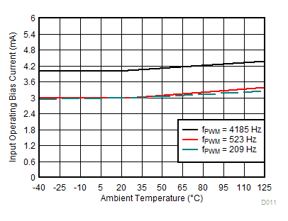
| IVIN-OP | Input operating bias current | No switching | 1 | mA | ||
| VIN-UVT | VIN internal POR threshold | VIN rising | 4.5 | V | ||
| VCC-REG | Regulated VCC voltage | 0 mA ≤ IVCC ≤ 5 mA | 3.1 | 3.3 | 3.5 | V |
| IVCC-LIM | VCC current limit | 10 | mA | |||
| VCPP | Charge pump operating voltage | VVIN = 5 V, VSW = 0 V – 60 V | 6.2 | V | ||
| fCPP | Charge pump oscillator frequency | 1.3 | 2.3 | 3.3 | MHz | |
| LED MATRIX SWITCHES | ||||||
| RDS(on) | LED switch on-resistance (2) | 225 | mΩ | |||
| RALL(on) | All switches on-resistance | Measured LED12 - LED0 | 1800 | 3400 | mΩ | |
| IDS(off) | OFF state switch leakage current | 50 | µA | |||
| VTH-S | LED short threshold voltage | VSW = 0 V – 60 V | 0.52 | 1.4 | V | |
| VTH-O | LED OPEN threshold voltage | VSW = 0 V – 60 V | 5 | 6 | 6.9 | V |
| tTO-O | LED OPEN detection and correction delay | 50 | 150 | ns | ||
| tREP | LED fault reporting delay | 5 | µs | |||
| tRISE(LEDx) | LEDx drain voltage rise time(1) | ILED = 800 mA | 2 | µs | ||
| tFALL(LEDx) | LEDx drain voltage fall time(1) | ILED = 800 mA | 2 | µs | ||
| DIGITAL SPECIFICATIONS | ||||||
| VIH-TH | High-level input voltage threshold | 1.9 | V | |||
| VIL-TH | Low-level input voltage threshold | 0.8 | V | |||
| VOH | High-level output voltage | ISOURCE = 2 mA, VVCC = 4.0 V | 4.27 | V | ||
| VOL | Low-level output voltage | ISINK = 2 mA, VVCC = 4.5 V | 0.23 | V | ||
| IOS | Output short circuit current (source or sink) | VVCC = 4.5 V | 42 | mA | ||
| RSP | Internal SYNC pull-down | 100 | kΩ | |||
| tWD-TO | CLK watchdog timeout | 32/fCPP | µs | |||
| tTO | CLK rise to TX output valid(1) | 80 | ns | |||
| tTZ | CLK rise to TX output tri-state(1) | 80 | ns | |||
(1) Specified by design. Not production tested.
(2) Single channel on-resitance (RDS(on)) measurement includes internal bond wires. All switches on-resistance (RALL(on)) should be used for all power calculations. See Internal Switch Resistance for details.
6.6 Typical Characteristics
TA = 25°C free air unless otherwise specified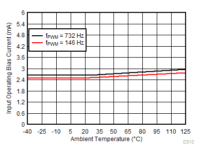
| VVIN = 5.5 V | fCLK = 6 MHz |
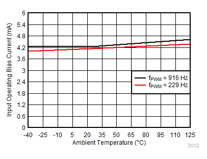
| VVIN = 5.5 V | fCLK = 15 MHz |
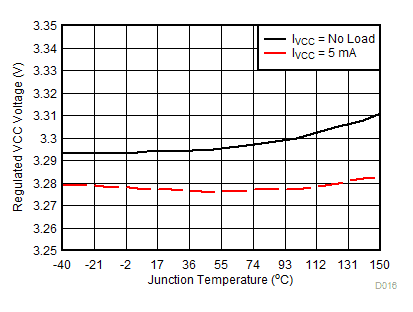
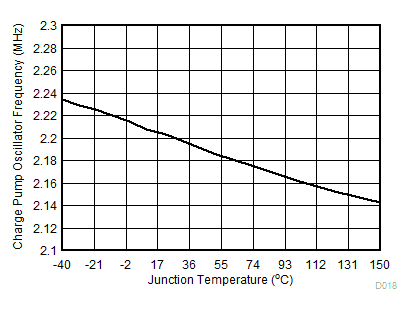 Figure 7. Charge Pump Oscillator Frequency vs Junction Temperature
| VVIN = 5.5 V | fCLK = 8.57 MHz |
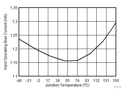
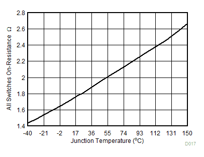
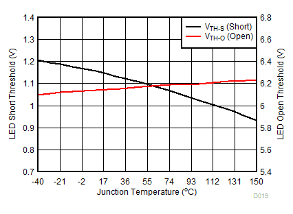 Figure 8. Channel Open and Short Protection Thresholds vs Junction Temperature