SLVSAD5A July 2010 – August 2015 TPS62120 , TPS62122
PRODUCTION DATA.
- 1 Features
- 2 Applications
- 3 Description
- 4 Revision History
- 5 Device Comparison Table
- 6 Pin Configuration and Functions
- 7 Specifications
- 8 Detailed Description
- 9 Application and Implementation
- 10Power Supply Recommendations
- 11Layout
- 12Device and Documentation Support
- 13Mechanical, Packaging, and Orderable Information
封裝選項(xiàng)
機(jī)械數(shù)據(jù) (封裝 | 引腳)
- DCN|8
散熱焊盤(pán)機(jī)械數(shù)據(jù) (封裝 | 引腳)
- DCN|8
訂購(gòu)信息
7 Specifications
7.1 Absolute Maximum Ratings
Over operating free-air temperature range (unless otherwise noted)(1)| MIN | MAX | UNIT | |||
|---|---|---|---|---|---|
| VI | Voltage at VIN(2) | –0.3 | 17 | V | |
| Voltage at SW PIN | dynamically during switching t < 10 µs | 17 | V | ||
| static DC | –0.3 | 6 | |||
| Voltage at EN PIN(2) | –0.3 | VIN +0.3, but ≤17 | V | ||
| Voltage on FB Pin | –0.3 | 3.6 | V | ||
| Voltage at PG, VOUT, SGND(2) | –0.3 | 6 | V | ||
| IIN | Current into PG pin | 0.5 | mA | ||
| Maximum operating junction temperature, TJ | –40 | 125 | °C | ||
| Storage temperature, Tstg | –65 | 150 | °C | ||
(1) Stresses beyond those listed under Absolute Maximum Ratings may cause permanent damage to the device. These are stress ratings only and functional operation of the device at these or any other conditions beyond those indicated under Recommended Operating Conditions is not implied. Exposure to absolute-maximum-rated conditions for extended periods may affect device reliability.
(2) All voltage values are with respect to network ground terminal GND.
7.2 ESD Ratings
| VALUE | UNIT | ||||
|---|---|---|---|---|---|
| V(ESD) | Electrostatic discharge | Human body model (HBM), per ANSI/ESDA/JEDEC JS-001(1) | ±2000 | V | |
| Charged device model (CDM), per JEDEC specification JESD22-C101(2) | ±1000 | ||||
(1) JEDEC document JEP155 states that 500-V HBM allows safe manufacturing with a standard ESD control process.
(2) JEDEC document JEP157 states that 250-V CDM allows safe manufacturing with a standard ESD control process.
7.3 Recommended Operating Conditions
| MIN | NOM | MAX | UNIT | ||
|---|---|---|---|---|---|
| Supply voltage VIN, device in operation | 2 | 15 | V | ||
| Output current capability | VIN = 2 V, VOUT = 1.8 V, DCRL = 0.7 Ω | 25 | mA | ||
| VIN ≥ 2.5 V, VOUT = 1.8 V, DCRL = 0.7 Ω | 75 | ||||
| Effective inductance | 10 | 22 | 33 | µH | |
| Effective output capacitance | 1.0 | 2 | 33 | µF | |
| Output voltage | 1.2 | 5.5 | V | ||
| Operating ambient temperature TA(1), (unless otherwise noted) | –40 | 85 | °C | ||
| Operating junction temperature, TJ | –40 | 125 | °C | ||
(1) In applications where high power dissipation and/or poor package thermal resistance is present, the maximum ambient temperature may have to be derated. Maximum ambient temperature (TA(max)) is dependent on the maximum operating junction temperature (TJ(max)), the maximum power dissipation of the device in the application (PD(max)), and the junction-to-ambient thermal resistance of the part/package in the application (RθJA), as given by the following equation: TA(max) = TJ(max) – (RθJA × PD(max)).
7.4 Thermal Information
| THERMAL METRIC(1) | TPS62120 | TPS62122 | UNIT | |
|---|---|---|---|---|
| DCN [SOT-23] | DRV [DFN] | |||
| 8 PINS | 6 PINS | |||
| RθJA | Junction-to-ambient thermal resistance | 259.7 | 114.4 | °C/W |
| RθJC(top) | Junction-to-case(top) thermal resistance | 114.1 | 73.7 | °C/W |
| RθJB | Junction-to-board thermal resistance | 185.8 | 201.9 | °C/W |
| ψJT | Junction-to-top characterization parameter | 21.6 | 0.8 | °C/W |
| ψJB | Junction-to-board characterization parameter | 121.6 | 94.9 | °C/W |
| RθJC(bot) | Junction-to-case(bottom) thermal resistance | n/a | 122.7 | °C/W |
(1) For more information about traditional and new thermal metrics, see the Semiconductor and IC PackageThermal Metrics application report, SPRA953
7.5 Electrical Characteristics
VIN = 8 V, VOUT = 1.8 V, EN = VIN, TJ = –40°C to 85°C, typical values are at TJ = 25°C (unless otherwise noted), CIN = 4.7 µF, L = 22 µH, COUT = 4.7 µF| PARAMETER | TEST CONDITIONS | MIN | TYP | MAX | UNIT | |
|---|---|---|---|---|---|---|
| SUPPLY | ||||||
| VIN | Input voltage range(1) | Device operating | 2 | 15 | V | |
| IQ | Quiescent current | IOUT = 0 mA, device not switching, EN = VIN, regulator sleeps | 11 | 18 | µA | |
| IOUT = 0 mA, device switching, VIN = 8 V, VOUT = 1.8 V | 13 | |||||
| IActive | Active mode current consumption | VIN = 5.5 V = VOUT, TJ = 25°C, high-side MOSFET switch fully turned on | 240 | 275 | µA | |
| ISD | Shutdown current | EN = GND, VOUT = SW = 0 V, VIN = 3.6 V (2) | 0.3 | 1.2 | µA | |
| VUVLO | Undervoltage lockout threshold | Falling VIN | 1.85 | 1.95 | V | |
| Rising VIN | 2.5 | 2.61 | ||||
| ENABLE, THRESHOLD | ||||||
| VIH TH | Threshold for detecting high EN | 2 V ≤ VIN ≤ 15 V, rising edge | 0.8 | 1.1 | V | |
| VIL TH HYS | Threshold for detecting low EN | 2 V ≤ VIN ≤ 15 V, falling edge | 0.4 | 0.6 | V | |
| IIN | Input bias current, EN | EN = GND or VIN | 0 | 50 | nA | |
| POWER SWITCH | ||||||
| RDS(ON) | High-side MOSFET ON-resistance | VIN = 3.6 V | 2.3 | 3.4 | Ω | |
| VIN = 8 V | 1.75 | 2.5 | ||||
| Low-side MOSFET ON-resistance | VIN = 3.6 V | 1.3 | 2.5 | |||
| VIN = 8 V | 1.2 | 1.75 | ||||
| ILIMF | Forward current limit MOSFET high-side | VIN = 8 V, open loop | 200 | 250 | 400 | mA |
| TSD | Thermal shutdown | Increasing junction temperature | 150 | °C | ||
| Thermal shutdown hysteresis | Decreasing junction temperature | 20 | °C | |||
| REGULATOR | ||||||
| tONmin | Minimum ON time | VIN = 3.6 V, VOUT = 1.8 V | 700 | ns | ||
| tOFFmin | Minimum OFF time | VIN = 3.6 V, VOUT = 1.8 V | 60 | ns | ||
| VREF | Internal reference voltage | 0.8 | V | |||
| VFB | Feedback FB voltage comparator threshold | Referred to 0.8-V internal reference | –2.5% | 0% | 2.5% | |
| Feedback FB voltage line regulation | IOUT = 50 mA (4) | 0.04 | %/V | |||
| IIN | Input bias current FB | VFB = 0.8 V | 0 | 50 | nA | |
| tStart | Regulator start-up time | Time from active EN to device starts switching, VIN = 2.6 V | 50 | 150 | µs | |
| tRamp | Output voltage ramp time | Time to ramp up VOUT = 1.8 V, no load (3) | 120 | 300 | ||
| ILK_SW | Leakage current into SW pin | VOUT = VIN = VSW = 1.8 V, EN = GND, device in shutdown mode | 1 | 1.5 | µA | |
| POWER GOOD OUTPUT (TPS62120) | ||||||
| VTHPG | Power good threshold voltage | Rising VFB feedback voltage | 93% | 95% | 97% | |
| Falling VFB feedback voltage | 87% | 90% | 93% | |||
| VOL | Output low voltage | Current into PG pin I = 500 µA, VOUT > 1.5 V | 165 | mV | ||
| Current into PG pin I = 100 µA, 1.2 V < VOUT < 1.5 V | 50 | |||||
| VH | Output high voltage | Open drain output, external pull up resistor | 5.5 | V | ||
| ILKG | Leakage current into PG pin | V(PG) = 1.8 V, EN = high, FB = 0.85 V | 0 | 50 | nA | |
| Leakage into VOUT pin | V(OUT) = 1.8 V | 0 | 50 | nA | ||
| TPGDL | Internal power good comparator delay time | VOUT = 1.8 V | 2 | 5 | µs | |
| SGND OPEN DRAIN OUTPUT (TPS62120) | ||||||
| RDS(ON) | NMOS drain source resistance | SGND = 1.8 V, VIN = 2 V | 370 | Ω | ||
| ILKG | Leakage current into SGND pin | EN = VIN, SGND = 1.8 V | 0 | 50 | nA | |
(1) The typical required supply voltage for startup is 2.5 V. The part is functional down to the falling UVLO (undervoltage lockout) threshold.
(2) Shutdown current into VIN pin, includes internal leakage.
(3) Maximum value not production tested.
(4) VOUT +1 V ≤ VIN ; VOUT ≤ 5.5 V
7.6 Typical Characteristics
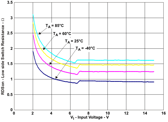 Figure 1. Low-Side Switch Resistance RDS(ON) vs VIN
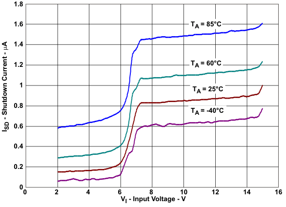 Figure 3. Shutdown Current vs VIN
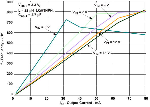 Figure 5. Switch Frequency vs Output Current IOUT
(VOUT = 3.3 V)
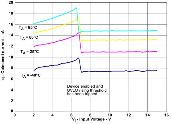 Figure 2. Quiescent Current vs VIN
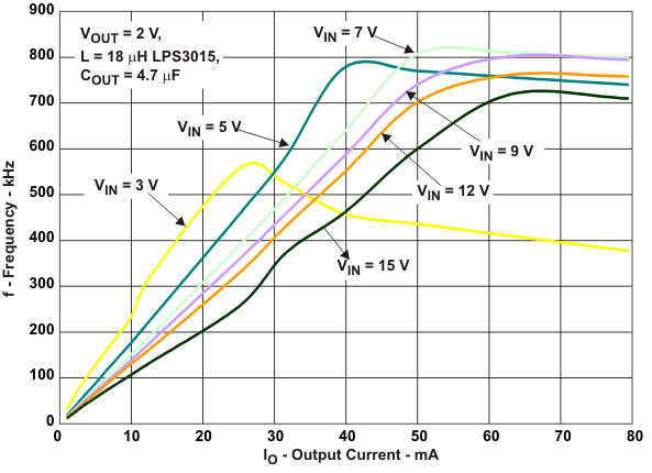 Figure 4. Switch Frequency vs Output Current IOUT
(VOUT = 2 V)
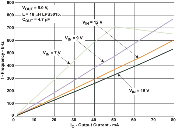 Figure 6. Switch Frequency vs Output Current IOUT
(VOUT = 5 V)