SLVS484C June 2003 – December 2014 TPS61090 , TPS61091 , TPS61092
PRODUCTION DATA.
- 1 Features
- 2 Applications
- 3 Description
- 4 Revision History
- 5 Device Comparison Table
- 6 Pin Configuration and Functions
- 7 Specifications
- 8 Parameter Measurement Information
- 9 Detailed Description
-
10Application and Implementation
- 10.1 Application Information
- 10.2
Typical Applications
- 10.2.1 Typical Application Circuit for Adjustable Output Voltage Option
- 10.2.2 TPS6109x Application Schematic of 5 Vout With Maximum Output Power
- 10.2.3 TPS6109x Application Schematic of 5 Vout and Auxiliary 10 Vout With Charge Pump
- 10.2.4 TPS6109x Application Schematic of 5 Vout and Auxiliary -5 Vout With Charge Pump
- 11Power Supply Recommendations
- 12Layout
- 13Device and Documentation Support
- 14Mechanical, Packaging, and Orderable Information
封裝選項(xiàng)
請(qǐng)參考 PDF 數(shù)據(jù)表獲取器件具體的封裝圖。
機(jī)械數(shù)據(jù) (封裝 | 引腳)
- RSA|16
散熱焊盤機(jī)械數(shù)據(jù) (封裝 | 引腳)
- RSA|16
訂購信息
7 Specifications
7.1 Absolute Maximum Ratings
over operating free-air temperature range (unless otherwise noted)(1)| MIN | MAX | UNIT | ||
|---|---|---|---|---|
| Input voltage on LBI | –0.3 | 3.6 | V | |
| Input voltage on SW, VOUT, LBO, VBAT, SYNC, EN, FB | –0.3 | 7 | V | |
| TA | Operating free air temperature | –40 | 85 | °C |
| TJ | Maximum junction temperature | 150 | °C | |
| Tstg | Storage temperature | –65 | 150 | °C |
(1) Stresses beyond those listed under Absolute Maximum Ratings may cause permanent damage to the device. These are stress ratings only, and functional operation of the device at these or any other conditions beyond those indicated under Recommended Operating Conditions is not implied. Exposure to absolute-maximum-rated conditions for extended periods may affect device reliability.
7.2 ESD Ratings
| VALUE | UNIT | |||
|---|---|---|---|---|
| V(ESD) | Electrostatic discharge | Human-body model (HBM), per ANSI/ESDA/JEDEC JS-001(1) | ±2000 | V |
| Charged-device model (CDM), per JEDEC specification JESD22-C101(2) | ±1000 | |||
(1) JEDEC document JEP155 states that 500-V HBM allows safe manufacturing with a standard ESD control process. Manufacturing with less than 500-V HBM is possible with the necessary precautions. Pins listed as ±XXX V may actually have higher performance.
(2) JEDEC document JEP157 states that 250-V CDM allows safe manufacturing with a standard ESD control process. Manufacturing with less than 250-V CDM is possible with the necessary precautions. Pins listed as ±YYY V may actually have higher performance.
7.3 Recommended Operating Conditions
| MIN | NOM | MAX | UNIT | ||
|---|---|---|---|---|---|
| VI | Supply voltage at VBAT | 1.8 | 5.5 | V | |
| L | Inductance | 2.2 | 6.8 | µH | |
| Ci | Input, capacitance | 10 | µF | ||
| Co | Output capacitance | 22 | 100 | ||
| TA | Operating free air temperature | –40 | 85 | °C | |
| TJ | Operating virtual junction temperature | –40 | 125 |
7.4 Electrical Characteristics
over recommended free-air temperature range and over recommended input voltage range (typical values are at an ambient temperature range of 25°C) (unless otherwise noted)| PARAMETER | TEST CONDITIONS | MIN | TYP | MAX | UNIT | ||
|---|---|---|---|---|---|---|---|
| DC-DC STAGE | |||||||
| VI | Input voltage range | 1.8 | 5.5 | V | |||
| VO | TPS61090 output voltage range | 1.8 | 5.5 | ||||
| VFB | TPS61090 feedback voltage | 490 | 500 | 510 | mV | ||
| f | Oscillator frequency | 500 | 600 | 700 | kHz | ||
| Frequency range for synchronization | 500 | 700 | |||||
| ISW | Switch current limit | VOUT= 5 V | 2000 | 2200 | 2500 | mA | |
| Start-up current limit | 0.4 x ISW | ||||||
| Boost switch on resistance | VOUT= 5 V | 55 | mΩ | ||||
| Rectifying switch on resistance | VOUT= 5 V | 55 | |||||
| Total accuracy | –3% | 3% | |||||
| Line regulation | 0.6% | ||||||
| Load regulation | 0.6% | ||||||
| Quiescent current | into VBAT | IO = 0 mA, VEN = VBAT = 1.8 V, VOUT =5 V | 10 | 25 | µA | ||
| into VOUT | IO = 0 mA, VEN = VBAT = 1.8 V, VOUT = 5 V | 10 | 20 | ||||
| Shutdown current | VEN= 0 V, VBAT = 2.4 V | 0.1 | 1 | ||||
| CONTROL STAGE | |||||||
| VUVLO | Under voltage lockout threshold | VLBI voltage decreasing | 1.5 | V | |||
| VIL | LBI voltage threshold | VLBI voltage decreasing | 490 | 500 | 510 | mV | |
| LBI input hysteresis | 10 | ||||||
| LBI input current | EN = VBAT or GND | 0.01 | 0.1 | µA | |||
| LBO output low voltage | VO = 3.3 V, IOI = 100 µA | 0.04 | 0.4 | V | |||
| LBO output low current | 100 | µA | |||||
| LBO output leakage current | VLBO = 7 V | 0.01 | 0.1 | ||||
| VIL | EN, SYNC input low voltage | 0.2 × VBAT | V | ||||
| VIH | EN, SYNC input high voltage | 0.8 × VBAT | |||||
| EN, SYNC input current | Clamped on GND or VBAT | 0.01 | 0.1 | µA | |||
| Overtemperature protection | 140 | °C | |||||
7.5 Typical Characteristics
Table 1. Table of Graphs
| DC-DC Converter | Figure | ||
|---|---|---|---|
| Maximum output current | vs Input voltage | Figure 1, Figure 2 | |
| Efficiency | vs Output current (TPS61090) (VO = 2.5 V, VI = 1.8 V, VSYNC = 0 V) | Figure 3 | |
| vs Output current (TPS61091) (VO = 3.3 V, VI = 1.8 V, 2.4 V, VSYNC = 0 V) | Figure 4 | ||
| vs Output current (TPS61092) (VO = 5.0 V, VI = 2.4 V, 3.3 V, VSYNC = 0 V) | Figure 5 | ||
| vs Output current (TPS61091) (IO = 10 mA, 100 mA, 500 mA, VSYNC = 0 V) | Figure 6 | ||
| vs Output current (TPS61092) (IO = 10 mA, 100 mA, 500 mA, VSYNC = 0 V) | Figure 7 | ||
| Output voltage | vs Output current (TPS61091) (VI = 2.4 V) | Figure 8 | |
| vs Output current (TPS61092) (VI = 3.3 V) | Figure 9 | ||
| No-load supply current into VBAT | Voltage (TPS61092) | Figure 10 | |
| No-load supply current into VOUT | vs Input voltage (TPS61092) | Figure 11 | |
| Minimum Load Resistance at Start-Up | vs Input Voltage (TPS61092) (VI = 3.3 V) | Figure 12 | |
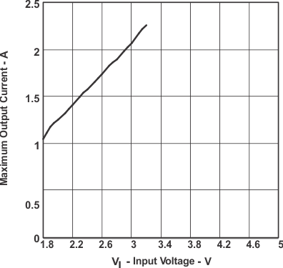 Figure 1. TPS61091 Maximum Output Current vs Input Voltage
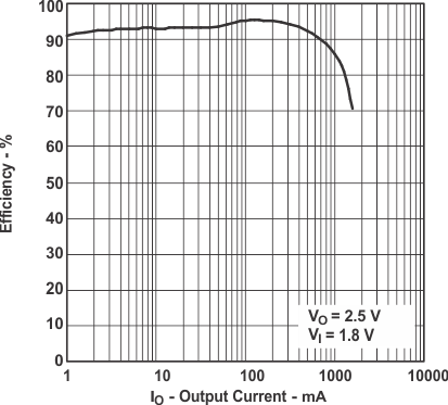 Figure 3. TPS61090 Efficiency vs Output Current
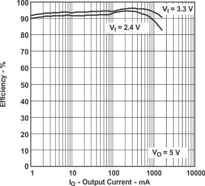 Figure 5. TPS61092 Efficiency vs Output Current
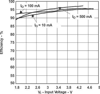 Figure 7. TPS61092 Efficiency vs Output Current
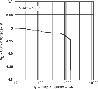 Figure 9. TPS61092 Output Voltage vs Output Current
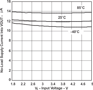 Figure 11. TPS61092 No-Load Supply Current Into VOUT vs Input Voltage
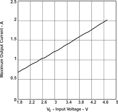 Figure 2. TPS61092 Maximum Output Current vs Input Voltage
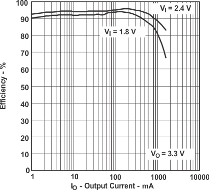 Figure 4. TPS61091 Efficiency vs Output Current
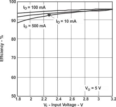 Figure 6. TPS61091 Efficiency vs Output Current
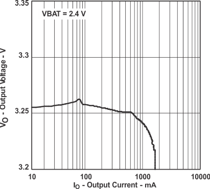 Figure 8. TPS61091 Efficiency vs Output Current
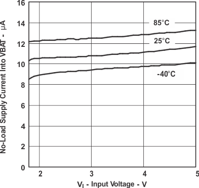 Figure 10. TPS61092 No-Load Supply Current Into VBAT Voltage
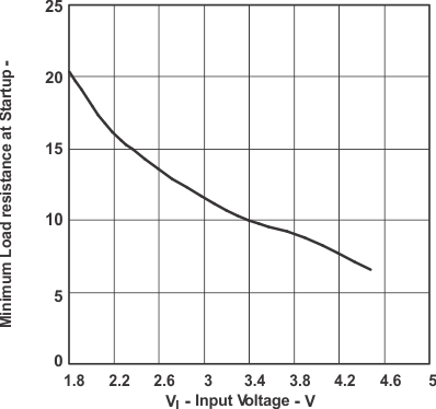 Figure 12. Minimum Load Resistance at Start-Up vs Input Voltage