SLVS484C June 2003 – December 2014 TPS61090 , TPS61091 , TPS61092
PRODUCTION DATA.
- 1 Features
- 2 Applications
- 3 Description
- 4 Revision History
- 5 Device Comparison Table
- 6 Pin Configuration and Functions
- 7 Specifications
- 8 Parameter Measurement Information
- 9 Detailed Description
-
10Application and Implementation
- 10.1 Application Information
- 10.2
Typical Applications
- 10.2.1 Typical Application Circuit for Adjustable Output Voltage Option
- 10.2.2 TPS6109x Application Schematic of 5 Vout With Maximum Output Power
- 10.2.3 TPS6109x Application Schematic of 5 Vout and Auxiliary 10 Vout With Charge Pump
- 10.2.4 TPS6109x Application Schematic of 5 Vout and Auxiliary -5 Vout With Charge Pump
- 11Power Supply Recommendations
- 12Layout
- 13Device and Documentation Support
- 14Mechanical, Packaging, and Orderable Information
封裝選項
請參考 PDF 數(shù)據(jù)表獲取器件具體的封裝圖。
機械數(shù)據(jù) (封裝 | 引腳)
- RSA|16
散熱焊盤機械數(shù)據(jù) (封裝 | 引腳)
- RSA|16
訂購信息
6 Pin Configuration and Functions
RSA Package
10 Pins
Top View
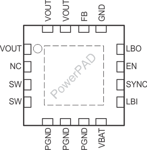
Pin Functions
| PIN | I/O | DESCRIPTION | |
|---|---|---|---|
| NAME | NO. | ||
| EN | 11 | I | Enable input. (1/VBAT enabled, 0/GND disabled) |
| FB | 14 | I | Voltage feedback of adjustable versions |
| GND | 13 | I/O | Control/logic ground |
| LBI | 9 | I | Low battery comparator input (comparator enabled with EN) |
| LBO | 12 | O | Low battery comparator output (open drain) |
| NC | 2 | Not connected | |
| PGND | 5, 6, 7 | I/O | Power ground |
| PowerPAD™ | — | — | Must be soldered to achieve appropriate power dissipation. Should be connected to PGND. |
| SYNC | 10 | I | Enable/disable power save mode (1: VBAT disabled, 0: GND enabled, clock signal for synchronization) |
| SW | 3, 4 | I | Boost and rectifying switch input |
| VBAT | 8 | I | Supply voltage |
| VOUT | 1, 15, 16 | O | DC-DC output |