SLVS859B June 2008 – December 2014 TPS61085
PRODUCTION DATA.
- 1 Features
- 2 Applications
- 3 Description
- 4 Simplified Schematic
- 5 Revision History
- 6 Pin Configuration and Functions
- 7 Specifications
- 8 Detailed Description
- 9 Application and Implementation
- 10Power Supply Recommendations
- 11Layout
- 12Device and Documentation Support
- 13Mechanical, Packaging, and Orderable Information
封裝選項
機械數(shù)據(jù) (封裝 | 引腳)
散熱焊盤機械數(shù)據(jù) (封裝 | 引腳)
訂購信息
7 Specifications
7.1 Absolute Maximum Ratings
over operating free-air temperature range (unless otherwise noted)(1)(2)| MIN | MAX | UNIT | |
|---|---|---|---|
| Input voltage range IN | –0.3 | 7 | V |
| Voltage range on pins EN, FB, SS, FREQ, COMP | –0.3 | 7 | V |
| Voltage on pin SW | -0.3 | 20 | V |
| Continuous power dissipation | See Thermal Information | ||
| Operating junction temperature | –40 | 150 | °C |
| Storage temperature | –65 | 150 | °C |
(1) Stresses beyond those listed under absolute maximum ratings may cause permanent damage to the device. These are stress ratings only, and functional operation of the device at these or any other conditions beyond those indicated under recommended operating conditions is not implied. Exposure to absolute-maximum-rated conditions for extended periods may affect device reliability
(2) All voltage values are with respect to network ground terminal.
7.2 ESD Ratings
| VALUE | UNIT | |||
|---|---|---|---|---|
| V(ESD) | Electrostatic discharge | Human body model (HBM), per ANSI/ESDA/JEDEC JS-001(1) | ±2000 | V |
| Charged-device model (CDM), per JEDEC specification JESD22-C101(2) | ±500 | |||
| Machine model (MM) | ±200 | |||
(1) JEDEC document JEP155 states that 500-V HBM allows safe manufacturing with a standard ESD control process. Manufacturing with less than 500-V HBM is possible with the necessary precautions. Pins listed as ±XXX V may actually have higher performance.
(2) JEDEC document JEP157 states that 250-V CDM allows safe manufacturing with a standard ESD control process. Manufacturing with less than 250-V CDM is possible with the necessary precautions. Pins listed as ±YYY V may actually have higher performance.
7.3 Recommended Operating Conditions
| MIN | TYP | MAX | UNIT | |||
|---|---|---|---|---|---|---|
| VIN | Input voltage range | 2.3 | 6 | V | ||
| VS | Boost output voltage range | VIN + 0.5 | 18.5 | V | ||
| TA | Operating free-air temperature | –40 | 85 | °C | ||
| TJ | Operating junction temperature | –40 | 125 | °C | ||
7.4 Thermal Information
| THERMAL METRIC(1) | TPS61085 | UNIT | ||
|---|---|---|---|---|
| DGK | PW | |||
| 8 PINS | 8 PINS | |||
| RθJA | Junction-to-ambient thermal resistance | 189.3 | 183.3 | °C/W |
| RθJC(top) | Junction-to-case (top) thermal resistance | 57.1 | 66.7 | |
| RθJB | Junction-to-board thermal resistance | 109.9 | 112.0 | |
| ψJT | Junction-to-top characterization parameter | 3.5 | 8.3 | |
| ψJB | Junction-to-board characterization parameter | 108.3 | 110.3 | |
(1) For more information about traditional and new thermal metrics, see the IC Package Thermal Metrics application report, SPRA953.
7.5 Electrical Characteristics
VIN = 3.3 V, EN = VIN, VS = 12 V, TA = –40°C to 85°C, typical values are at TA = 25°C (unless otherwise noted)| PARAMETER | TEST CONDITIONS | MIN | TYP | MAX | UNIT | |
|---|---|---|---|---|---|---|
| SUPPLY | ||||||
| VIN | Input voltage range | 2.3 | 6 | V | ||
| IQ | Operating quiescent current into IN | Device not switching, VFB = 1.3 V | 70 | 100 | μA | |
| ISDVIN | Shutdown current into IN | EN = GND | 1 | μA | ||
| UVLO | Undervoltage lockout threshold | VIN falling | 2.2 | V | ||
| VIN rising | 2.3 | V | ||||
| TSD | Thermal shutdown | Temperature rising | 150 | °C | ||
| TSD(HYS) | Thermal shutdown hysteresis | 14 | °C | |||
| LOGIC SIGNALS EN, FREQ | ||||||
| VIH | High level input voltage | VIN = 2.3 V to 6 V | 2 | V | ||
| VIL | Low level input voltage | VIN = 2.3 V to 6 V | 0.5 | V | ||
| Ilkg | Input leakage current | EN = FREQ = GND | 0.1 | μA | ||
| BOOST CONVERTER | ||||||
| VS | Boost output voltage | VIN + 0.5 | 18.5 | V | ||
| VFB | Feedback regulation voltage | 1.230 | 1.238 | 1.246 | V | |
| gm | Transconductance error amplifier | 107 | μA/V | |||
| IFB | Feedback input bias current | VFB = 1.238 V | 0.1 | μA | ||
| rDS(on) | N-channel MOSFET on-resistance | VIN = VGS = 5 V, ISW = current limit | 0.13 | 0.20 | Ω | |
| VIN = VGS = 3.3V, ISW = current limit | 0.15 | 0.24 | ||||
| Ilkg | SW leakage current | EN = GND, VSW = 6V TBD | 10 | µA | ||
| ILIM | N-Channel MOSFET current limit | 2.0 | 2.6 | 3.2 | A | |
| ISS | Soft-start current | VSS = 1.238 V | 7 | 10 | 13 | μA |
| fS | Oscillator frequency | FREQ = VIN | 0.9 | 1.2 | 1.5 | MHz |
| FREQ = GND | 480 | 650 | 820 | kHz | ||
| Line regulation | VIN = 2.3 V to 6 V, IOUT = 10 mA | 0.0002 | %/V | |||
| Load regulation | VIN = 3.3 V, IOUT = 1 mA to 400 mA | 0.11 | %/A | |||
7.6 Typical Characteristics
The typical characteristics are measured with the inductors 7447789003 3.3 µH (high frequency) or B82464G4 6.8 µH (low frequency) from Epcos and the rectifier diode SL22.Table 1. Table Of Graphs
| FIGURE | |||
|---|---|---|---|
| IOUT(max) | Maximum load current | vs Input voltage at high frequency (1.2 MHz) | Figure 1 |
| vs Input voltage at low frequency (650 kHz) | Figure 2 | ||
| η | Efficiency | vs Load current, VS = 12 V, VIN = 3.3 V | Figure 3 |
| vs Load current, VS = 9 V, VIN = 3.3 V | Figure 4 | ||
| Supply current | vs Supply voltage | Figure 5 | |
| Frequency | vs Load current | Figure 6 | |
| Frequency | vs Supply voltage | Figure 7 | |
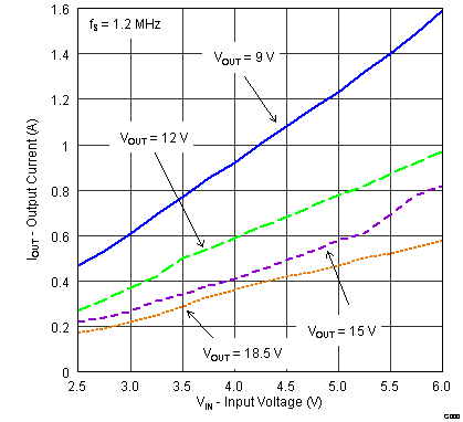 Figure 1. Maximum Load Current vs Input Voltage
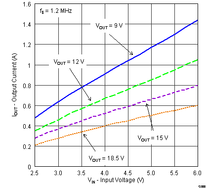 Figure 2. Maximum Load Current vs Input Voltage
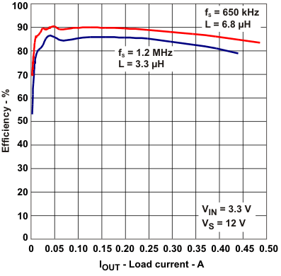 Figure 3. Efficiency vs Load Current
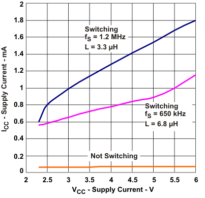 Figure 5. Supply Current vs Supply Voltage
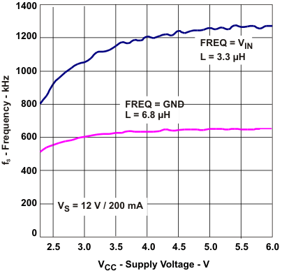 Figure 7. Frequency vs Supply Voltage
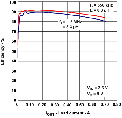 Figure 4. Efficiency vs Load Current
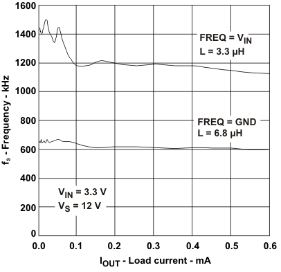 Figure 6. Frequency vs Load Current