ZHCSFR5 November 2016 TPS562210A , TPS563210A
PRODUCTION DATA.
- 1 特性
- 2 應(yīng)用
- 3 說(shuō)明
- 4 修訂歷史記錄
- 5 Pin Configuration and Functions
- 6 Specifications
- 7 Detailed Description
- 8 Application and Implementation
- 9 Power Supply Recommendations
- 10Layout
- 11器件和文檔支持
- 12機(jī)械、封裝和可訂購(gòu)信息
封裝選項(xiàng)
機(jī)械數(shù)據(jù) (封裝 | 引腳)
- DDF|8
散熱焊盤(pán)機(jī)械數(shù)據(jù) (封裝 | 引腳)
訂購(gòu)信息
5 Pin Configuration and Functions
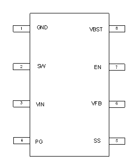
DDF Package
8 Pin
Top View

Pin Functions
| PIN | DESCRIPTION | |
|---|---|---|
| NAME | NO. | |
| GND | 1 | Ground pin Source terminal of low-side power NFET as well as the ground terminal for controller circuit. Connect sensitive VFB to this GND at a single point. |
| SW | 2 | Switch node connection between high-side NFET and low-side NFET. |
| VIN | 3 | Input voltage supply pin. The drain terminal of high-side power NFET. |
| PG | 4 | Power good open drain output |
| SS | 5 | Soft-start control. An external capacitor should be connected to GND. |
| VFB | 6 | Converter feedback input. Connect to output voltage with feedback resistor divider. |
| EN | 7 | Enable input control. Active high and must be pulled up to enable the device. |
| VBST | 8 | Supply input for the high-side NFET gate drive circuit. Connect 0.1 µF capacitor between VBST and SW pins. |