ZHCSBX1B NOVEMBER 2013 – December 2014 TPS53915
PRODUCTION DATA.
- 1 特性
- 2 應(yīng)用范圍
- 3 說(shuō)明
- 4 修訂歷史記錄
- 5 Pin Configuration and Functions
- 6 Specifications
-
7 Detailed Description
- 7.1 Overview
- 7.2 Functional Block Diagrams
- 7.3
Feature Description
- 7.3.1 Powergood
- 7.3.2 D-CAP3 Control and Mode Selection
- 7.3.3 D-CAP3 Mode
- 7.3.4 Sample and Hold Circuitry
- 7.3.5 Adaptive Zero-Crossing
- 7.3.6 Forced Continuous-Conduction Mode
- 7.3.7 Current Sense and Overcurrent Protection
- 7.3.8 Overvoltage and Undervoltage Protection
- 7.3.9 Out-Of-Bounds Operation (OOB)
- 7.3.10 UVLO Protection
- 7.3.11 Thermal Shutdown
- 7.4 Device Functional Modes
- 7.5
Programming
- 7.5.1 The PMBus General Descriptions
- 7.5.2 PMBus Slave Address Selection
- 7.5.3 PMBus Address Selection
- 7.5.4 Supported Formats
- 7.5.5 Supported PMBus Commands
- 7.5.6 CLEAR_FAULTS [03h] (Send Byte)
- 7.5.7 STORE_DEFAULT_ALL [11h] (Send Byte)
- 7.5.8 RESTORE_DEFAULT_ALL [12h] (Send Byte)
- 7.5.9 STATUS_WORD [79h] (Read Word)
- 7.5.10 CUSTOM_REG (MFR_SPECIFIC_00) [D0h] (R/W Byte)
- 7.5.11 DELAY_CONTROL (MFR_SPECIFIC_01) [D1h] (R/W Byte)
- 7.5.12 MODE_SOFT_START_CONFIG (MFR_SPECIFIC_02) [D2h] (R/W Byte)
- 7.5.13 FREQUENCY_CONFIG (MFR_SPECIFIC_03) [D3h] (R/W Byte)
- 7.5.14 VOUT_ADJUSTMENT (MFR_SPECIFIC_04) [D4h] (R/W Byte)
- 7.5.15 Output Voltage Fine Adjustment Soft Slew Rate
- 7.5.16 VOUT_MARGIN (MFR_SPECIFIC_05) [D5h] (R/W Byte)
- 7.5.17 Output Voltage Margin Adjustment Soft-Slew Rate
- 7.5.18 UVLO_THRESHOLD (MFR_SPECIFIC_06) [D6h]
- 8 Application and Implementation
- 9 Power Supply Recommendations
- 10Layout
- 11器件和文檔支持
- 12機(jī)械、封裝和可訂購(gòu)信息
封裝選項(xiàng)
機(jī)械數(shù)據(jù) (封裝 | 引腳)
- RVE|28
散熱焊盤(pán)機(jī)械數(shù)據(jù) (封裝 | 引腳)
- RVE|28
訂購(gòu)信息
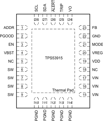
5 Pin Configuration and Functions
28-PIN
QFN
(TOP VIEW)

Pin Functions(1)
| PIN | I/O | DESCRIPTION | |
|---|---|---|---|
| NAME | NO. | ||
| ADDR | 1 | I | PMBus address configuration pin. Connect this pin into a resistor divider between VREG and GND to program different address settings |
| ALERT | 26 | O | Alert output for the PMBus interface |
| EN | 3 | I | The enable pin turns on the DC-DC switching converter. |
| FB | 23 | I | VOUT feedback input. Connect this pin to a resistor divider between the VOUT pin and GND. |
| GND | 22 | G | This pin is the ground of internal analog circuitry and driver circuitry. Connect GND to the PGND plane with a short trace (For example, connect this pin to the thermal pad with a single trace and connect the thermal pad to PGND pins and PGND plane). |
| MODE | 21 | I | The MODE pin sets the forced continuous-conduction mode (FCCM) or Skip-mode operation. It also selects the ramp coefficient of D-CAP3 mode. |
| NC | 5 | — | Not connected. These pins are floating internally. |
| 18 | |||
| PGND | 10 | G | These ground pins are connected to the return of the internal low-side MOSFET. |
| 11 | |||
| 12 | |||
| 13 | |||
| 14 | |||
| PGOOD | 2 | O | Open-drain power-good status signal which provides startup delay after the FB voltage falls within the specified limits. After the FB voltage moves outside the specified limits, PGOOD goes low within 2 µs. |
| SCL | 28 | I | Clock input for the PMBus interface |
| SDA | 27 | I/O | Data I/O for the PMBus interface |
| SW | 6 | I/O | SW is the output switching terminal of the power converter. Connect this pin to the output inductor. |
| 7 | |||
| 8 | |||
| 9 | |||
| TRIP | 25 | I/O | TRIP is the OCL detection threshold setting pin. ITRIP = 10 µA at TA = 25°C, 3000 ppm/°C current is sourced and sets the OCL trip voltage. See the Current Sense and Overcurrent Protection section for detailed OCP setting. |
| VBST | 4 | P | VBST is the supply rail for the high-side gate driver (boost terminal). Connect the bootstrap capacitor from this pin to the SW node. Internally connected to VREG via bootstrap PMOS switch. |
| VDD | 19 | P | Power-supply input pin for controller. Input of the VREG LDO. The input range is from 4.5 to 25 V. |
| VIN | 15 | P | VIN is the conversion power-supply input pins. |
| 16 | |||
| 17 | |||
| VREG | 20 | O | VREG is the 5-V LDO output. This voltage supplies the internal circuitry and gate driver. |
| VO | 24 | I | VOUT voltage input to the controller. |
(1) I = Input, O = Output, P = Supply, G = Ground