SLVSA55B November 2009 – November 2016 TPD4S1394
PRODUCTION DATA.
- 1 Features
- 2 Applications
- 3 Description
- 4 Revision History
- 5 Pin Configuration and Functions
- 6 Specifications
- 7 Detailed Description
- 8 Application and Implementation
- 9 Power Supply Recommendations
- 10Layout
- 11Device and Documentation Support
- 12Mechanical, Packaging, and Orderable Information
封裝選項(xiàng)
機(jī)械數(shù)據(jù) (封裝 | 引腳)
- DQL|8
散熱焊盤(pán)機(jī)械數(shù)據(jù) (封裝 | 引腳)
- DQL|8
訂購(gòu)信息
6 Specifications
6.1 Absolute Maximum Ratings
over operating free-air temperature range (unless otherwise noted)(1)| MIN | MAX | UNIT | ||
|---|---|---|---|---|
| VCC | Supply voltage | –0.5 | 4.6 | V |
| VIO | IO voltage at D+, D–, VCLMP | 0 | 4 | V |
| FWPWR_EN | Switch output | –0.5 | 4.6 | V |
| TA | Operating free-air temperature | –40 | 85 | °C |
| Tstg | Storage temperature | –65 | 150 | °C |
(1) Stresses beyond those listed under Absolute Maximum Ratings may cause permanent damage to the device. These are stress ratings only, which do not imply functional operation of the device at these or any other conditions beyond those indicated under Recommended Operating Conditions. Exposure to absolute-maximum-rated conditions for extended periods may affect device reliability.
6.2 ESD Ratings
| VALUE | UNIT | ||||
|---|---|---|---|---|---|
| V(ESD) | Electrostatic discharge | Human-body model (HBM), per ANSI/ESDA/JEDEC JS-001(1) | All pins except 5, 6, 7, and 8 | ±2500 | V |
| Pins 5, 6, 7, and 8 | ±15000 | ||||
| Charged-device model (CDM), per JEDEC specification JESD22-C101(2) | All pins except 5, 6, 7, and 8 | ±1000 | |||
| Pins 5, 6, 7, and 8 | ±1000 | ||||
| IEC 61000-4-2 contact discharge | Pins 5, 6, 7, and 8 (interface side) | ±6000 | |||
| IEC 61000-4-2 air-gap discharge | Pins 5, 6, 7, and 8 (interface side) | ±6000 | |||
(1) JEDEC document JEP155 states that 500-V HBM allows safe manufacturing with a standard ESD control process.
(2) JEDEC document JEP157 states that 250-V CDM allows safe manufacturing with a standard ESD control process.
6.3 Recommended Operating Conditions
over operating free-air temperature range (unless otherwise noted)| PARAMETER | MIN | MAX | UNIT | |
|---|---|---|---|---|
| VCC | Supply voltage | 3 | 3.6 | V |
6.4 Thermal Information
| THERMAL METRIC(1) | TPD4S1394 | UNIT | |
|---|---|---|---|
| DQL (X2SON) | |||
| 8 PINS | |||
| RθJA | Junction-to-ambient thermal resistance | 167.5 | °C/W |
| RθJC(top) | Junction-to-case (top) thermal resistance | 56.8 | °C/W |
| RθJB | Junction-to-board thermal resistance | 82.3 | °C/W |
| ψJT | Junction-to-top characterization parameter | 1.5 | °C/W |
| ψJB | Junction-to-board characterization parameter | 82 | °C/W |
(1) For more information about traditional and new thermal metrics, see the Semiconductor and IC Package Thermal Metrics application report.
6.5 Electrical Characteristics
over operating free-air temperature range (unless otherwise noted)(1)| PARAMETER | TEST CONDITIONS | MIN | TYP | MAX | UNIT | ||
|---|---|---|---|---|---|---|---|
| VDX | FWPWR_EN trip voltage (D+ and D– pins) |
High-to-low | 2.9 | 3.4 | 4 | V | |
| Low-to-high | 2.7 | 3.2 | 3.8 | ||||
| VCLMP | Value on pin | No connection | 2.45 | V | |||
| VBR | Breakdown voltage at VCLAMP | II = 1 mA | 4.2 | V | |||
| VD | Diode forward voltage for lower clamp | ID = 8 mA lower clamp diode | –0.6 | –0.8 | –0.95 | V | |
| FWPWR_EN | Switch output | VCC | V | ||||
| RDYN | Dynamic resistance (in and out clamp) of D+, D– | I = 1 A | 1 | Ω | |||
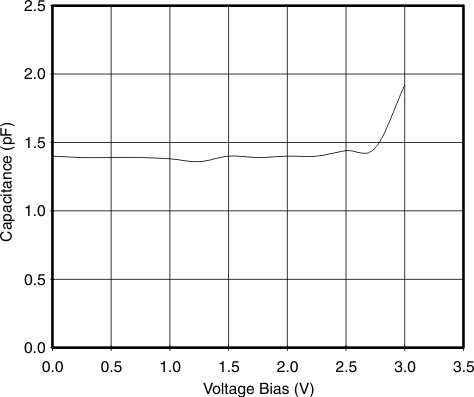
| CIO | I/O capacitance of D+, D– | VIO = 2.5 V | 1.5 | 2 | pF | ||
| ICC | Current consumption | VCC = 3.3 V, FWPWR_EN = high | 130 | 200 | µA | ||
(1) A 0.1-µF decoupling capacitor is required at VCC.
6.6 Switching Characteristics
over operating free-air temperature range (unless otherwise noted)| PARAMETER | TEST CONDITIONS | MIN | TYP | MAX | UNIT | |
|---|---|---|---|---|---|---|
| tTRIP | Delay time for FWPWR_EN to go low | Loading on FWPWR_EN = 50 pF | 0.5 | 2 | 5 | µs |
| tRESET | Delay time for FWPWR_EN to go high after trip | FWPWR_EN = VCC | 300 | 450 | 600 | ms |
6.7 Typical Characteristics

| D+, D– Pins |

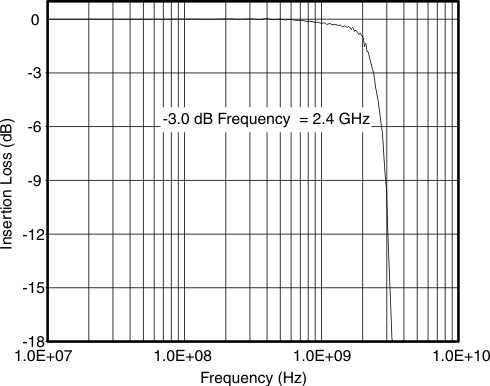
| D+, D– Pins |