ZHCSL40N November 2004 – June 2024 TLVH431 , TLVH431A , TLVH431B , TLVH432 , TLVH432A , TLVH432B
PRODUCTION DATA
- 1
- 1 特性
- 2 應(yīng)用
- 3 說明
- 4 Pin Configuration and Functions
- 5 Specifications
- 6 Parameter Measurement Information
- 7 Detailed Description
- 8 Applications and Implementation
- 9 Device and Documentation Support
- 10Revision History
- 11Mechanical, Packaging, and Orderable Information
封裝選項(xiàng)
機(jī)械數(shù)據(jù) (封裝 | 引腳)
散熱焊盤機(jī)械數(shù)據(jù) (封裝 | 引腳)
- PK|3
訂購信息
5.8 Typical Characteristics
Operation of the device at these or any other conditions beyond those indicated in the Section 5.3 table are not implied.
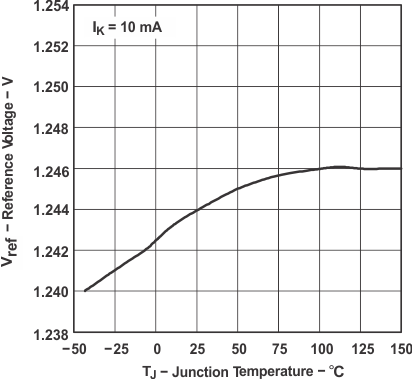 Figure 5-1 Reference Voltage vs Junction Temperature
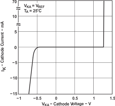 Figure 5-3 Cathode Current vs Cathode Voltage
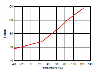 Figure 5-5 Minimum Cathode Current vs. Temperature
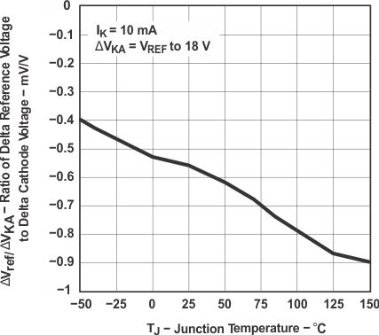
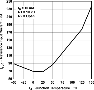
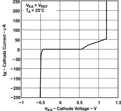 Figure 5-4 Cathode Current vs Cathode Voltage
 Figure 5-6 Off-State Cathode Current vs Junction Temperature
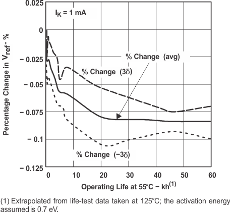 Figure 5-8 Percentage Change in VREF vs Operating Life at 55°C
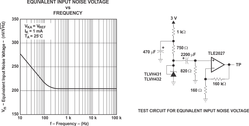 Figure 5-9 Equivalent Input Noise Voltage
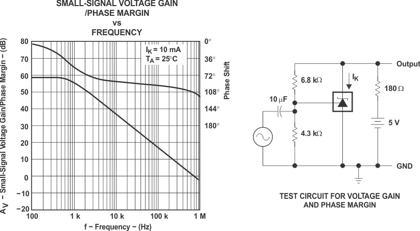 Figure 5-11 Voltage Gain and Phase Margin
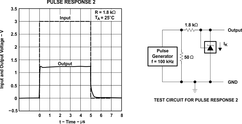 Figure 5-13 Pulse
Response 2
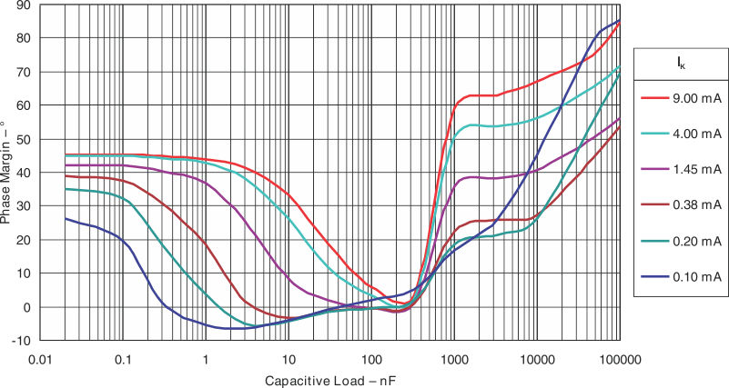 Figure 5-15 Phase
Margin vs Capacitive Load VKA = VREF (1.25 V),
TA= 25°C
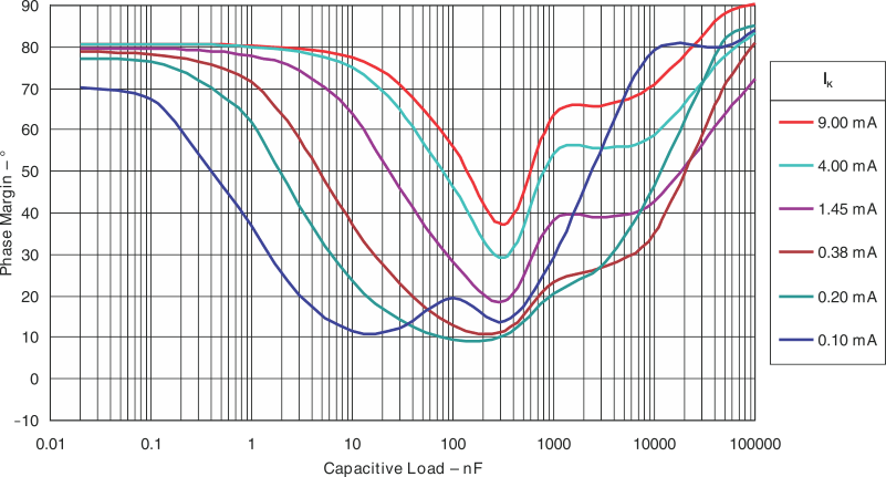 Figure 5-17 Phase
Margin vs Capacitive Load VKA = 5.00V, TA=
25°C
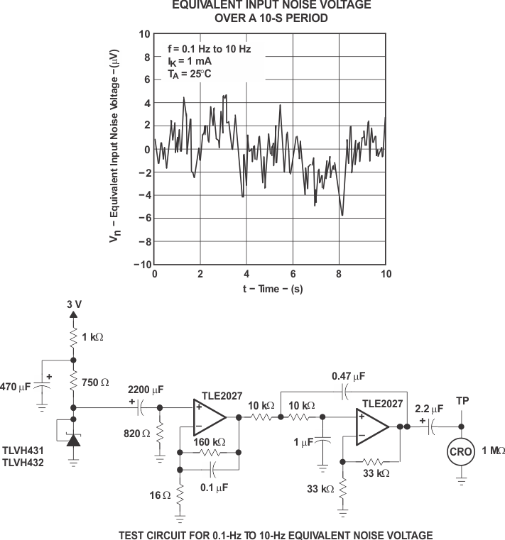
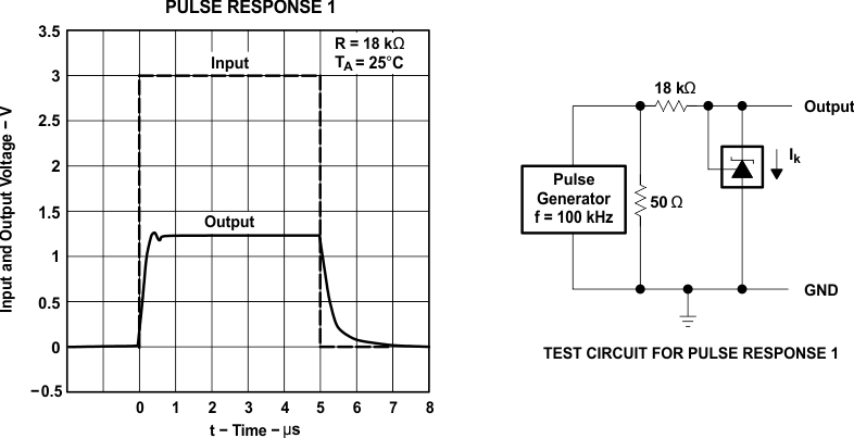 Figure 5-12 Pulse
Response 1
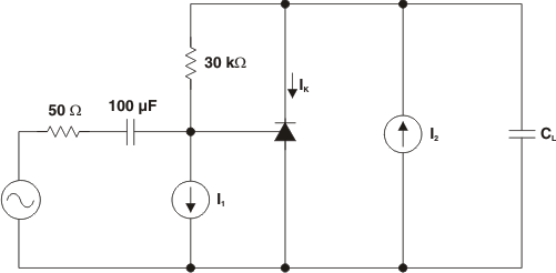 Figure 5-14 Phase
Margin Test Circuit
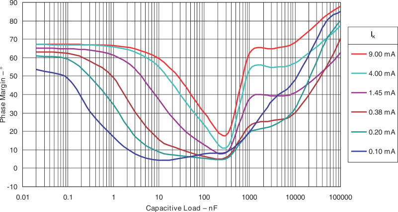 Figure 5-16 Phase
Margin vs Capacitive Load VKA = 2.50V, TA=
25°C