ZHCSEG6F December 2015 – May 2025 TCAN330 , TCAN330G , TCAN332 , TCAN332G , TCAN334 , TCAN334G , TCAN337 , TCAN337G
PRODUCTION DATA
- 1
- 1特性
- 2應(yīng)用
- 3說(shuō)明
- Device Options
- 4Pin Configuration and Functions
- 5Specifications
- Parameter Measurement Information
- 6Detailed Description
- 7Application Information Disclaimer
- Device and Documentation Support
- 8Revision History
- 9Mechanical, Packaging, and Orderable Information
封裝選項(xiàng)
機(jī)械數(shù)據(jù) (封裝 | 引腳)
散熱焊盤(pán)機(jī)械數(shù)據(jù) (封裝 | 引腳)
- DCN|8
訂購(gòu)信息
5.6 Switching Characteristics
over operating free-air temperature range (unless otherwise noted)
| PARAMETER | TEST CONDITIONS | MIN | TYP | MAX | UNIT | |
|---|---|---|---|---|---|---|
| Device Switching Characteristics | ||||||
| tPROP(LOOP) | Total loop delay, driver input (TXD) to receiver output (RXD), recessive to dominant and dominant to recessive | See Figure 6-6, S, STB and SHDN = 0V, RL = 60?, CL = 100pF, CL(RXD) = 15pF | 100 | 135 | ns | |
| tPROP(LOOP) | Total Loop delay in highly loaded network | See Figure 6-6, S, STB and SHDN = 0V, RL = 120?, CL =
200pF, CL(RXD) = 15pF | 120 | 180 | ns | |
| tBUS_SYM_2 | 2 Mbps transmitted recessive bit width | See Figure 6-7, S or STB = 0V, RL = 60?, CL = 100pF,
CL(RXD) = 15 pF, tBIT = 500ns TCAN330G, TCAN332G, TCAN334G and TCAN337G only | 435 | 530 | ns | |
| tREC_SYM_2 | 2 Mbps received recessive bit width | 400 | 550 | ns | ||
| ΔtSYM_2 | 2 Mbps receiver timing symmetry (tREC_SYM_2 - tBUS_SYM_2) | –65 | 40 | ns | ||
| tBUS_SYM_5 | 5 Mbps transmitted recessive bit width | See Figure 6-7, S or STB = 0V, RL = 60?, CL = 100pF,
CL(RXD) = 15pF, tBIT = 200ns TCAN330G, TCAN332G, TCAN334G and TCAN337G only | 155 | 210 | ns | |
| tREC_SYM_5 | 5 Mbps received recessive bit width | 120 | 220 | ns | ||
| ΔtSYM_5 | 5 Mbps receiver timing symmetry (tREC_SYM_5 - tBUS_SYM_5) | –45 | 15 | ns | ||
| tMODE | Mode change time | See Figure 6-4 and Figure 6-5. RL = 60Ω, CL = 100pF, CL(RXD) = 15pF | 5 | 10 | μs | |
| tUV_RE-ENABLE | Re-enable time after UV event | Time for device to return to normal operation from UV(VCC) under voltage event | 1000 | μs | ||
| tWK_FILTER | Bus time to meet Filtered Bus Requirements for Wake Up Request | See Figure 6-5, Standby mode. –12V < VCM < 12V | 0.5 | 4 | μs | |
| Driver Switching Characteristics | ||||||
| tpHR | Propagation delay time, HIGH TXD to Driver Recessive | See Figure 6-2, S, STB and SHDN = 0V. RL = 60?, CL = 100pF, | 25 | ns | ||
| tpLD | Propagation delay time, LOW TXD to Driver Dominant | 20 | ||||
| tsk(p) | Pulse skew (|tpHR - tpLD|) | 5 | ||||
| tr | Differential output signal rise time | 17 | ||||
| tf | Differential output signal fall time | 9 | ||||
| tTXD_DTO | Driver dominant time out (1) | See Figure 6-8, RL = 60Ω, CL = 100pF | 1.2 | 2.6 | 3.8 | ms |
| Receiver Switching Characteristics | ||||||
| tpRH | Propagation delay time, bus recessive input to high RXD output | See Figure 6-3, CL(RXD) = 15pF CANL = 1.5V, CANH = 3.5V | 62 | ns | ||
| tpDL | Propagation delay time, bus dominant input to RXD low output | 56 | ||||
| tr | Output signal rise time (RXD) | 7 | ||||
| tf | Output signal fall time (RXD) | 6 | ||||
| tRXD_DTO | Receiver dominant time out (2) | See Figure 6-10, CL(RXD) = 15pF | 1.6 | 3 | 5 | ms |
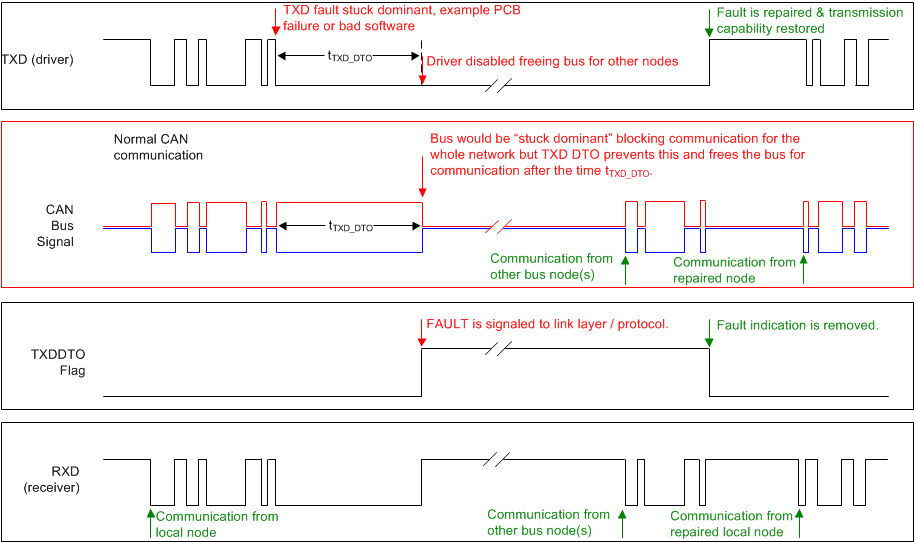
(1) The TXD dominant time out (tTXD_DTO) disables the driver of the
transceiver once the TXD has been dominant longer than tTXD_DTO,
which releases the bus lines to recessive, preventing a local failure from
locking the bus dominant. The driver may only transmit dominant again after TXD
has been returned HIGH (recessive). While this protects the bus from local
faults, locking the bus dominant, it limits the minimum data rate possible. The
CAN protocol allows a maximum of eleven successive dominant bits (on TXD) for
the worst case, where five successive dominant bits are followed immediately by
an error frame. This, along with the tTXD_DTO minimum, limits the
minimum bit rate. The minimum bit rate may be calculated by: Minimum Bit Rate =
11/ tTXD_DTO = 11 bits / 1.2 ms = 9.2kbps.
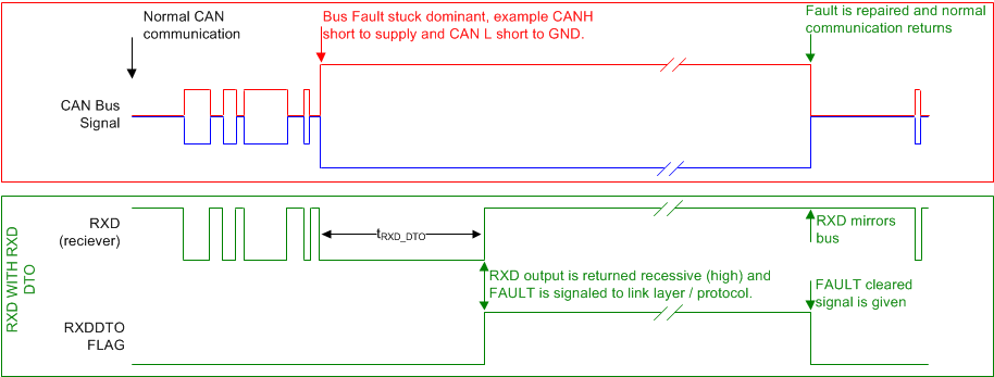
(2) The RXD timeout (tRXD_DTO) disables the RXD output in the case that
the bus has been dominant longer than tRXD_DTO, which releases RXD
pin to the recessive state (high), thus preventing a dominant bus failure from
permanently keeping the RXD pin low. The RXD pin will automatically resume
normal operation once the bus has been returned to a recessive state. While this
protects the protocol controller from a permanent dominant state, it limits the
minimum data rate possible. The CAN protocol allows a maximum of eleven
successive dominant bits (on RXD) for the worst case, where five successive
dominant bits are followed immediately by an error frame. This, along with the
tRXD_DTO minimum, limits the minimum bit rate. The minimum bit
rate may be calculated by: Minimum Bit Rate = 11 / tRXD_DTO = 11 bits
/ 1.6ms = 6.9kbps.
 Figure 5-1 Example Timing Diagram for TXD DTO and FAULT Pin
 Figure 5-2 Example Timing Diagram for RXD DTO and FAULT Pin