ZHCSMK1I February 2008 – February 2025 SN74AVC4T774
PRODUCTION DATA
- 1
- 1 特性
- 2 應(yīng)用
- 3 說明
- 4 Pin Configuration and Functions
-
5 Specifications
- 5.1 Absolute Maximum Ratings
- 5.2 ESD Ratings
- 5.3 Recommended Operating Conditions
- 5.4 Thermal Information
- 5.5 Electrical Characteristics
- 5.6 Switching Characteristics: VCCA = 1.2V ± 0.1V
- 5.7 Switching Characteristics: VCCA = 1.5V ± 0.1V
- 5.8 Switching Characteristics: VCCA = 1.8V ± 0.15V
- 5.9 Switching Characteristics: VCCA = 2.5V ± 0.2V
- 5.10 Switching Characteristics: VCCA = 3.3V ± 0.3V
- 5.11 Typical Characteristics
- 6 Parameter Measurement Information
- 7 Detailed Description
- 8 Application and Implementation
- 9 Device and Documentation Support
- 10Revision History
- 11Mechanical, Packaging, and Orderable Information
封裝選項(xiàng)
機(jī)械數(shù)據(jù) (封裝 | 引腳)
散熱焊盤機(jī)械數(shù)據(jù) (封裝 | 引腳)
訂購信息
4 Pin Configuration and Functions

A. Shown for a single channel
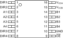
Figure 4-1 PW Package, 16-Pin TSSOP (Top View)
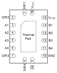
 Figure 4-3 RGY Package, 16-Pin VQFN
 (Top View)
Figure 4-2 DYY Package, 16-Pin SOT
(Top View)
(Top View)
 Figure 4-4 RSV Package, 16-Pin UQFN
 (Top View)
 Figure 4-5 BQB Package, 16-Pin WQFN, Transparent
 (Top View)
Table 4-1 Pin Functions
| PIN | TYPE | DESCRIPTION | ||
|---|---|---|---|---|
| NAME | PW, RGY BQB, DYY | RSV | ||
| DIR1 | 1 | 15 | I | Direction-control input referenced to VCCA, controls signal flow for the first (A1/B1) I/O channels. |
| DIR2 | 2 | 16 | I | Direction-control input referenced to VCCA , controls signal flow for the second (A2/B2) I/O channels. |
| A1 | 3 | 1 | I/O | Input/output A1. Referenced to VCCA. |
| A2 | 4 | 2 | I/O | Input/output A2. Referenced to VCCA. |
| A3 | 5 | 3 | I/O | Input/output A3. Referenced to VCCA. |
| A4 | 6 | 4 | I/O | Input/output A4. Referenced to VCCA. |
| DIR3 | 7 | 5 | I | Direction-control input referenced to VCCA , controls signal flow for the third (A3/B3) I/O channels. |
| DIR4 | 8 | 6 | I | Direction-control input referenced to VCCA , controls signal flow for the fourth (A4/B4) I/O channels. |
| OE | 9 | 7 | I | 3-state output-mode enables. Pull OE high to place all outputs in 3-state mode. Referenced to VCCA. |
| GND | 10 | 8 | — | Ground. |
| B4 | 11 | 9 | I/O | Input/output B4. Referenced to VCCB. |
| B3 | 12 | 10 | I/O | Input/output B3. Referenced to VCCB. |
| B2 | 13 | 11 | I/O | Input/output B2. Referenced to VCCB. |
| B1 | 14 | 12 | I/O | Input/output B1. Referenced to VCCB. |
| VCCB | 15 | 13 | — | B-port supply voltage. 1.1V ≤ VCCB ≤ 3.6V. |
| VCCA | 16 | 14 | — | A-port supply voltage. 1.1V ≤ VCCA ≤ 3.6V. |