SLES254D April 2010 – July 2015 PCM1753-Q1 , PCM1754-Q1
PRODUCTION DATA.
- 1 Features
- 2 Applications
- 3 Description
- 4 Revision History
- 5 Device Comparison Table
- 6 Pin Configuration Functions
- 7 Specifications
-
8 Detailed Description
- 8.1 Overview
- 8.2 Functional Block Diagram
- 8.3 Feature Description
- 8.4 Device Functional Modes
- 8.5 Programming
- 8.6
Register Maps
- 8.6.1
Mode Control Registers (PCM1753-Q1)
- 8.6.1.1 User-Programmable Mode Controls
- 8.6.1.2
Register Definitions
- 8.6.1.2.1 ATx[7:0]: Digital Attenuation Level Setting
- 8.6.1.2.2 MUTx: Soft Mute Control
- 8.6.1.2.3 OVER: Oversampling Rate Control
- 8.6.1.2.4 SRST: Reset
- 8.6.1.2.5 DACx: DAC Operation Control
- 8.6.1.2.6 DM12: Digital De-Emphasis Function Control
- 8.6.1.2.7 DMF[1:0]: Sampling Frequency Selection for the De-Emphasis Function
- 8.6.1.2.8 FMT[2:0]: Audio Interface Data Format
- 8.6.1.2.9 FLT: Digital Filter Rolloff Control
- 8.6.1.2.10 DREV: Output Phase Select
- 8.6.1.2.11 ZREV: Zero Flag Polarity Select
- 8.6.1.2.12 AZRO: Zero Flag Function Select
- 8.6.1
Mode Control Registers (PCM1753-Q1)
- 9 Application and Implementation
- 10Power Supply Recommendations
- 11Layout
- 12Device and Documentation Support
- 13Mechanical, Packaging, and Orderable Information
封裝選項(xiàng)
機(jī)械數(shù)據(jù) (封裝 | 引腳)
- DBQ|16
散熱焊盤機(jī)械數(shù)據(jù) (封裝 | 引腳)
訂購(gòu)信息
7 Specifications
7.1 Absolute Maximum Ratings
over operating free-air temperature range (unless otherwise noted)(1)| MIN | MAX | UNIT | ||
|---|---|---|---|---|
| Supply voltage | VCC | –0.3 | 6.5 | V |
| Ground voltage differences | AGND, DGND | –0.1 | 0.1 | V |
| Input voltage | –0.3 | 6.5 | V | |
| Input current (any pins except supplies) | –10 | 10 | mA | |
| Ambient temperature under bias | –40 | 105 | °C | |
| Junction temperature | 150 | °C | ||
| Storage temperature, Tstg | –55 | 150 | °C | |
(1) Stresses beyond those listed under Absolute Maximum Ratings may cause permanent damage to the device. These are stress ratings only, and functional operation of the device at these or any other conditions beyond those indicated is not implied. Exposure to absolute-maximum-rated conditions for extended periods may affect device reliability.
7.2 ESD Ratings
| VALUE | UNIT | ||||
|---|---|---|---|---|---|
| V(ESD) | Electrostatic discharge | Human body model (HBM), per AEC Q100–002(1) | ±2000 | V | |
| Charged device model (CDM), per AEC Q100–011 | Corner pins (1, 8, 9, and 16) | ±750 | |||
| Other pins | ±500 | ||||
(1) AEC Q100–002 indicates HBM stressing is done in accordance with the ANSI/ESDA/JEDEC JS–001 specification.
7.3 Recommended Operating Conditions
over operating free-air temperature range (unless otherwise noted)| MIN | NOM | MAX | UNIT | ||
|---|---|---|---|---|---|
| VCC | Voltage range | 4.5 | 5 | 5.5 | VDC |
7.4 Thermal Information
| THERMAL METRIC(1) | PCM175x-Q1 | UNIT | |
|---|---|---|---|
| DBQ (SSOP) | |||
| 16 PINS | |||
| RθJA | Junction-to-ambient thermal resistance | 111.8 | °C/W |
| RθJC(top) | Junction-to-case (top) thermal resistance | 57.4 | °C/W |
| RθJB | Junction-to-board thermal resistance | 55.1 | °C/W |
| ψJT | Junction-to-top characterization parameter | 13.5 | °C/W |
| ψJB | Junction-to-board characterization parameter | 54.6 | °C/W |
| RθJC(bot) | Junction-to-case (bottom) thermal resistance | N/A | °C/W |
(1) For more information about traditional and new thermal metrics, see the Semiconductor and IC Package Thermal Metrics application report, SPRA953.
7.5 Electrical Characteristics
All specifications at TA = 25°C, VCC = 5 V, fS = 44.1 kHz, system clock = 384 fS, and 24-bit data (unless otherwise noted)| PARAMETER | TEST CONDITIONS | MIN | TYP | MAX | UNIT | ||
|---|---|---|---|---|---|---|---|
| Resolution | 24 | Bits | |||||
| DATA FORMAT | |||||||
| fS | Sampling frequency | 5 | 200 | kHz | |||
| System clock frequency(3) | 128 fS
192 fS 256 fS 384 fS 512 fS 768 fS 1152 fS |
kHz | |||||
| DIGITAL INPUT/OUTPUT | |||||||
| Logic family | TTL compatible | ||||||
| VIH | Input logic level, high | 2 | VDC | ||||
| VIL | Input logic level, low | 0.8 | |||||
| IIH | Input logic current, high (SCK, BCK, DATA, and LRCK pins) | VIN = VCC | 10 | µA | |||
| IIL | Input logic current, low (SCK, BCK, DATA, and LRCK pins) | VIN = 0 V | –10 | µA | |||
| IIH | Input logic current, high (TEST, DEMP, MUTE, and FMT pins) | VIN = VCC | 65 | 100 | µA | ||
| IIL | Input logic current, low (TEST, DEMP, MUTE, and FMT pins) | VIN = 0 V | –10 | µA | |||
| VOH | Output logic level, high (ZEROA pin) | IOH = –1 mA | 2.4 | VDC | |||
| VOL | Output logic level, low (ZEROA pin) | IOL = 1 mA | 0.4 | VDC | |||
| DYNAMIC PERFORMANCE(1)(2) | |||||||
| THD+N at VOUT = 0 dB | fS = 44.1 kHz | 0.00% | 0.01% | ||||
| fS = 96 kHz | 0.00% | ||||||
| fS = 192 kHz | 0.00% | ||||||
| THD+N at VOUT = -60 dB | fS = 44.1 kHz | 0.65% | |||||
| fS = 96 kHz | 0.80% | ||||||
| fS = 192 kHz | 0.95% | ||||||
| Dynamic range | EIAJ, A-weighted, fS = 44.1 kHz | 100 | 106 | dB | |||
| A-weighted, fS = 96 kHz | 104 | ||||||
| A-weighted, fS = 192 kHz | 102 | ||||||
| Signal-to-noise ratio | EIAJ, A-weighted, fS = 44.1 kHz | 100 | 106 | dB | |||
| A-weighted, fS = 96 kHz | 104 | ||||||
| A-weighted, fS = 192 kHz | 102 | ||||||
| Channel separation | fS = 44.1 kHz | 97 | 103 | dB | |||
| fS = 96 kHz | 101 | ||||||
| fS = 192 kHz | 100 | ||||||
| Level linearity error | VOUT = -90 dB | ±0.5 | dB | ||||
| DC ACCURACY | |||||||
| Gain error | ±1 | ±6 | % of FSR | ||||
| Gain mismatch, channel-to-channel | ±1 | ±3 | % of FSR | ||||
| Bipolar zero error | VOUT = 0.5 VCC at BPZ | ±30 | ±60 | mV | |||
| ANALOG OUTPUT | |||||||
| Output voltage | Full scale (0 dB) | 80% of VCC | VPP | ||||
| Center voltage | 50% of VCC | VDC | |||||
| Load impedance | AC-coupled load | 5 | kΩ | ||||
| DIGITAL FILTER PERFORMANCE | |||||||
| FILTER CHARACTERISTICS (SHARP ROLLOFF) | |||||||
| Pass band | ±0.04 dB | 0.454 fS | |||||
| Stop band | 0.546 fs | ||||||
| Pass-band ripple | ±0.04 | dB | |||||
| Stop-band attenuation | Stop band = 0.546 fS | –50 | dB | ||||
| ANALOG FILTER PERFORMANCE | |||||||
| Frequency response | At 20 kHz | –0.03 | dB | ||||
| At 44 kHz | –0.20 | ||||||
| POWER SUPPLY REQUIREMENTS(2) | |||||||
| VCC | Voltage range | 4.5 | 5 | 5.5 | VDC | ||
| ICC | Supply current | fS = 44.1 kHz | 16 | 21 | mA | ||
| fS = 96 kHz | 25 | ||||||
| fS = 192 kHz | 30 | ||||||
| Power dissipation | fS = 44.1 kHz | 80 | 105 | mW | |||
| fS = 96 kHz | 125 | ||||||
| fS = 192 kHz | 150 | ||||||
| TEMPERATURE RANGE | |||||||
| Operation temperature | –40 | 105 | °C | ||||
| RθJA | Thermal resistance | 16-pin SSOP | 115 | °C/W | |||
(1) Analog performance specifications are measured using the System Two™ Cascade audio measurement system by Audio Precision™ in the averaging mode.
(2) Conditions in 192-kHz operation are system clock = 128 fS and oversampling rate = 64 fS of register 18.
(3) System Clock: 128 fS, 192 fS, 256 fS, 384 fS, 512 fS, 768 fS, 1152 fS with auto detect.
7.6 System Clock Input Timing
For more information, see the System Clock Input section.| MIN | NOM | MAX | UNIT | |||
|---|---|---|---|---|---|---|
| t(SCKH) | System clock pulse duration, high | See Figure 20. | 7 | ns | ||
| t(SCKL) | System clock pulse duration, low | 7 | ns | |||
| t(SCY) | System clock pulse cycle time | See (1) | ns | |||
(1) 1/128 fS, 1/256 fS, 1/384 fS, 1/512 fS, 1/768 fS, or 1/1152 fS
7.7 Audio Interface Timing
For more information, see the Audio Data Formats and Timing section.| MIN | MAX | UNIT | |||
|---|---|---|---|---|---|
| t(BCY) | BCK pulse cycle time | See Figure 22. | 1/(32 fS) 1/(48 fS) 1/(64 fS)(1) |
ns | |
| t(BCH) | BCK high–level time | 35 | ns | ||
| t(BCL) | BCK low–level time | 35 | ns | ||
| t(BL) | BCK rising edge to LRCK edge | 10 | ns | ||
| t(LB) | LRCK falling edge to BCK rising edge | 10 | ns | ||
| t(DS) | DATA setup time | 10 | ns | ||
| t(DH) | DATA hold time | 10 | ns | ||
(1) fS is the sampling frequency (such as, 44.1 kHz, 48 kHz, 96 kHz, and so on).
7.8 Control Interface Timing Requirements
These timing parameters are critical for proper control port operation.| MIN | NOM | MAX | UNIT | |||
|---|---|---|---|---|---|---|
| t(MCY) | MC pulse cycle time | See Figure 1. | 100 | ns | ||
| t(MCL) | MC low-level time | 50 | ns | |||
| t(MCH) | MC high-level time | 50 | ns | |||
| t(MCH) | ML high-level time | See (2) | ns | |||
| t(MLS) | ML falling edge to MC rising edge | 20 | ns | |||
| t(MLH) | ML hold time(1) | 20 | ns | |||
| t(MDH) | MD hold time | 15 | ns | |||
| t(MDS) | MD setup time | 20 | ns | |||
(1) MC rising edge for LSB to ML rising edge.
(2)  seconds (min); fS: sampling rate.
 seconds (min); fS: sampling rate.
 Figure 1. Control Interface Timing
7.9 Typical Characteristics
7.9.1 Digital Filter (De-Emphasis Off)
All specifications at TA = 25°C, VCC = 5 V, fS = 44.1 kHz, system clock = 384 fS, and 24-bit data, (unless otherwise noted)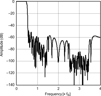
| Frequency response | Sharp rolloff | |
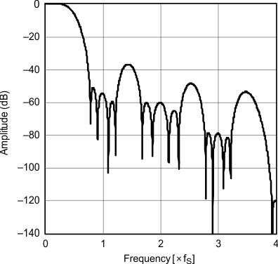
| Frequency response | Slow rolloff | |
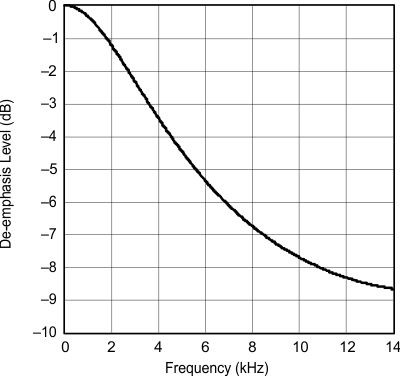
| fS = 32 kHz |
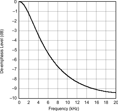
| fS = 44.1 kHz |
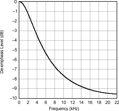
| fS = 48 kHz |
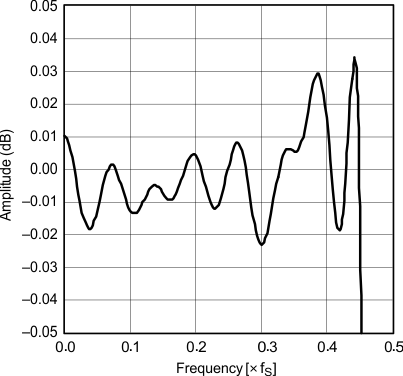
| Pass-band ripple | Sharp rolloff | |
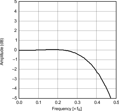
| Transition characteristics | Slow rolloff | |
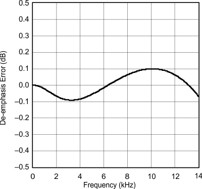
| fS = 32 kHz |
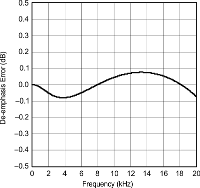
| fS = 44.1 kHz |
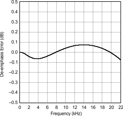
| fS = 48 kHz |
7.9.2 Analog Dynamic Performance (Supply Voltage Characteristics)
All specifications at TA = 25°C, VCC = 5 V, fS = 44.1 kHz, system clock = 384 fS, and 24-bit data, (unless otherwise noted)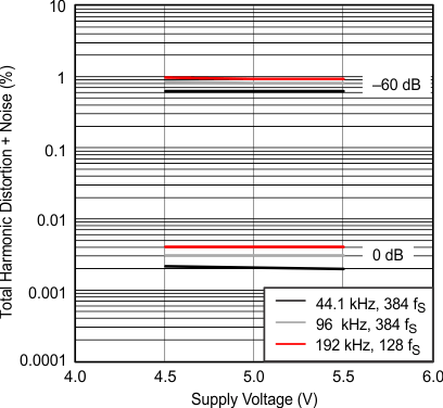 Figure 12. Total Harmonic Distortion + Noise vs Supply Voltage
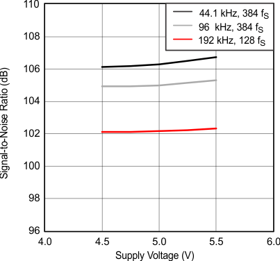 Figure 14. Signal-to-Noise Ratio vs Supply Voltage
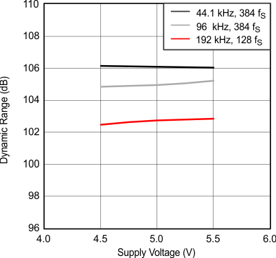 Figure 13. Dynamic Range vs Supply Voltage
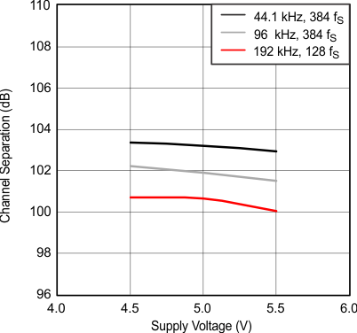 Figure 15. Channel Separation vs Supply Voltage
7.9.3 Analog Dynamic Performance (Temperature Characteristics)
All specifications at TA = 25°C, VCC = 5 V, fS = 44.1 kHz, system clock = 384 fS, and 24-bit data, (unless otherwise noted) Figure 16. Total Harmonic Distortion + Noise vs Free-Air Temperature
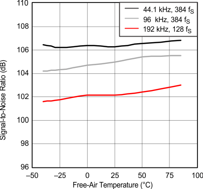 Figure 18. Signal-to-Noise Ratio vs Free-Air Temperature
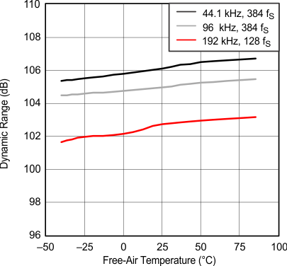 Figure 17. Dynamic Range vs Free-Air Temperature
 Figure 19. Channel Separation vs Free-Air Temperature