ZHCSNI8J September 2006 – March 2021 PCA9534A
PRODUCTION DATA
- 1 特性
- 2 說明
- 3 Revision History
- 4 Description (Continued)
- 5 Device Comparison Table
- 6 Pin Configuration and Functions
- 7 Specifications
- 8 Parameter Measurement Information
- 9 Detailed Description
- 10Application Information Disclaimer
- 11Power Supply Recommendations
- 12Device and Documentation Support
- 13Mechanical, Packaging, and Orderable Information
封裝選項
機械數(shù)據(jù) (封裝 | 引腳)
散熱焊盤機械數(shù)據(jù) (封裝 | 引腳)
訂購信息
6 Pin Configuration and Functions
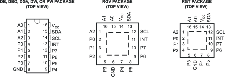
Table 6-1 Pin Functions
| PIN | DESCRIPTION | ||
|---|---|---|---|
| NAME | QSOP (DBQ), SOIC (DW), SSOP (DB), TSSOP (PW), AND TVSOP (DGV) |
QFN (RGT) AND QFN (RGV) |
|
| A0 | 1 | 15 | Address input. Connect directly to VCC or ground. |
| A1 | 2 | 16 | Address input. Connect directly to VCC or ground. |
| A2 | 3 | 1 | Address input. Connect directly to VCC or ground. |
| P0 | 4 | 2 | P-port input/output. Push-pull design structure. |
| P1 | 5 | 3 | P-port input/output. Push-pull design structure. |
| P2 | 6 | 4 | P-port input/output. Push-pull design structure. |
| P3 | 7 | 5 | P-port input/output. Push-pull design structure. |
| GND | 8 | 6 | Ground |
| P4 | 9 | 7 | P-port input/output. Push-pull design structure. |
| P5 | 10 | 8 | P-port input/output. Push-pull design structure. |
| P6 | 11 | 9 | P-port input/output. Push-pull design structure. |
| P7 | 12 | 10 | P-port input/output. Push-pull design structure. |
| INT | 13 | 11 | Interrupt output. Connect to VCC through a pullup resistor. |
| SCL | 14 | 12 | Serial clock bus. Connect to VCC through a pullup resistor. |
| SDA | 15 | 13 | Serial data bus. Connect to VCC through a pullup resistor. |
| VCC | 16 | 14 | Supply voltage |