ZHCS590Q January 2011 – December 2014 LMP90097 , LMP90098 , LMP90099 , LMP90100
PRODUCTION DATA.
- 1 特性
- 2 應(yīng)用
- 3 說明
- 4 典型應(yīng)用電路原理圖
- 5 修訂歷史記錄
- 6 說明(續(xù))
- 7 Pin Configuration and Functions
- 8 Specifications
-
9 Detailed Description
- 9.1 Overview
- 9.2 Functional Block Diagram
- 9.3
Feature Description
- 9.3.1 True Continuous Background Calibration
- 9.3.2 Continuous Background Sensor Diagnostics
- 9.3.3 Flexible Input MUX Channels
- 9.3.4 Programmable Gain Amplifiers (FGA and PGA)
- 9.3.5 Excitation Current Sources (IB1 and IB2) - LMP90100/LMP90098
- 9.3.6 Signal Path
- 9.3.7 Calibration
- 9.3.8 Sensor Interface
- 9.3.9 RESET and RESTART
- 9.4 Device Functional Modes
- 9.5
Programming
- 9.5.1 General Rules
- 9.5.2 Serial Digital Interface
- 9.5.3 Register Address (ADDR)
- 9.5.4 Register Read/Write Protocol
- 9.5.5 Streaming
- 9.5.6 CSB - Chip Select Bar
- 9.5.7 SPI Reset
- 9.5.8 DRDYB - Data Ready Bar
- 9.5.9 DRDYB Case1: Combining SDO/DRDYB with SDO_DRDYB_DRIVER = 0x00
- 9.5.10 DRDYB Case2: Combining SDO/DRDYB with SDO_DRDYB_DRIVER = 0x03
- 9.5.11 DRDYB Case3: Routing DRDYB to D6
- 9.5.12 Data Only Read Transaction
- 9.5.13 Cyclic Redundancy Check (CRC)
- 9.5.14 Register Read/Write Examples
- 9.5.15 Streaming Examples
- 9.6 Register Maps
- 10Application and Implementation
- 11Power Supply Recommendations
- 12Layout
- 13器件和文檔支持
- 14機械封裝和可訂購信息
封裝選項
機械數(shù)據(jù) (封裝 | 引腳)
- PWP|28
散熱焊盤機械數(shù)據(jù) (封裝 | 引腳)
- PWP|28
訂購信息
7 Pin Configuration and Functions
HTSSOP (PWP0028A) PACKAGE
28 PINS
TOP VIEW
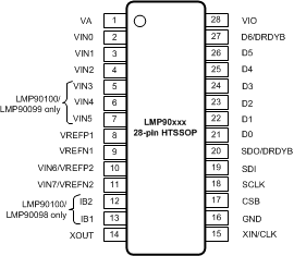
See below for specific information regarding options LMP90099, LMP90098, and LMP90097.
Pin Functions
| PIN | TYPE | DESCRIPTION | |
|---|---|---|---|
| NAME | NO. | ||
| VA | 1 | Analog Supply | Analog power supply pin |
| VIN0 to VIN2 | 2 to 4 | Analog Input | Analog input pins |
| VIN3 to VIN5 | 5 to 7 (LMP90100, LMP90099 only) |
Analog Input | Analog input pins |
| VIN3 to VIN5 | 5 - 7 (LMP90098, LMP90097 only) |
No Connect | No connect: must be left unconnected |
| VREFP1 | 8 | Analog Input | Positive reference input |
| VREFN1 | 9 | Analog Input | Negative reference input |
| VIN6 / VREFP2 | 10 | Analog Input | Analog input pin or VREFP2 input |
| VIN7 / VREFN2 | 11 | Analog Input | Analog input pin or VREFN2 input |
| IB2, IB1 | 12 to 13 (LMP90100, LMP90098 only) |
Analog Output | Excitation current sources for external RTDs |
| IB2, IB1 | 12 - 13 (LMP90099, LMP90097 only) |
No Connect | No connect: must be left unconnected |
| XOUT | 14 | Analog Output | External crystal oscillator connection |
| XIN / CLK | 15 | Analog Input | External crystal oscillator connection or external clock input |
| GND | 16 | Ground | Power supply ground |
| CSB | 17 | Digital Input | Chip select bar |
| SCLK | 18 | Digital Input | Serial clock |
| SDI | 19 | Digital Input | Serial data input |
| SDO / DRDYB | 20 | Digital Output | Serial data output and data ready bar |
| D0 to D5 | 21 to 26 | Digital IO | General purpose input/output (GPIO) pins |
| D6 / DRDYB | 27 | Digital IO | General purpose input/output pin or data ready bar |
| VIO | 28 | Digital Supply | Digital input/output supply pin |
| Thermal Pad | — | — | You can leave this thermal pad floating. |