SNOS469J April 2000 – January 2015 LM8261
PRODUCTION DATA.
- 1 Features
- 2 Applications
- 3 Description
- 4 Revision History
- 5 Pin Configuration and Functions
- 6 Specifications
- 7 Application and Implementation
- 8 Power Supply Recommendations
- 9 Layout
- 10Device and Documentation Support
- 11Mechanical, Packaging, and Orderable Information
封裝選項(xiàng)
機(jī)械數(shù)據(jù) (封裝 | 引腳)
- DBV|5
散熱焊盤(pán)機(jī)械數(shù)據(jù) (封裝 | 引腳)
訂購(gòu)信息
6 Specifications
6.1 Absolute Maximum Ratings(1)
| MIN | MAX | UNIT | ||
|---|---|---|---|---|
| VIN Differential | ±10 | V | ||
| Output Short Circuit Duration | See(3)(5) | |||
| Supply Voltage (V+ - V−) | 32 | V | ||
| Voltage at Input/Output pins | V+ +0.8 V, V− −0.8 V |
V | ||
| Storage Temperature Range | −65 | +150 | °C | |
| Junction Temperature(4) | 150 | °C | ||
| Soldering Information: | Infrared or Convection (20 sec.) | 235 | °C | |
| Wave Soldering (10 sec.) | 260 | °C | ||
(1) Absolute Maximum Ratings indicate limits beyond which damage to the device may occur. Operating Rating indicate conditions for which the device is intended to be functional, but specific performance is not guaranteed. For guaranteed specifications and the test conditions, see Electrical Characteristics 2.7 V.
(2) Human Body Model is 1.5 kΩ in series with 100 pF.
(3) Applies to both single-supply and split-supply operation. Continuous short circuit operation at elevated ambient temperature can result in exceeding the maximum allowed junction temperature of 150°C.
(4) The maximum power dissipation is a function of TJ(max), RθJA, and TA. The maximum allowable power dissipation at any ambient temperature is PD = (TJ(MAX) - TA)/ RθJA. All numbers apply for packages soldered directly onto a PC board.
(5) Allowable Output Short Circuit duration is infinite for VS ≤ 6 V at room temperature and below. For VS > 6 V, allowable short circuit duration is 1.5 ms.
(6) Machine Model, 0 Ω is series with 200 pF.
6.2 ESD Ratings
| VALUE | UNIT | |||
|---|---|---|---|---|
| V(ESD) | Electrostatic discharge | Human-body model (HBM), per ANSI/ESDA/JEDEC JS-001(1)(2) | ±2000 | V |
| Machine model (MM)(6) | ±200 | |||
(1) JEDEC document JEP155 states that 500-V HBM allows safe manufacturing with a standard ESD control process. Manufacturing with less than 2000-V HBM is possible with the necessary precautions. Pins listed as ±200 V may actually have higher performance.
6.3 Recommended Operating Conditions
| MIN | MAX | UNIT | ||
|---|---|---|---|---|
| Supply Voltage (V+ - V−) | 2.5 | 30 | V | |
| Temperature Range(2) | −40 | +85 | °C | |
6.4 Thermal Information
| THERMAL METRIC(1)(2) | DBV | UNIT | |
|---|---|---|---|
| (5 PINS) | |||
| RθJA | Junction-to-ambient thermal resistance | 325 | °C/W |
(1) For more information about traditional and new thermal metrics, see the IC Package Thermal Metrics application report, SPRA953.
(2) The maximum power dissipation is a function of TJ(max), RθJA, and TA. The maximum allowable power dissipation at any ambient temperature is PD = (TJ(MAX) - TA)/ RθJA. All numbers apply for packages soldered directly onto a PC board.
6.5 Electrical Characteristics 2.7 V
Unless otherwise specified, all limits guaranteed for TA = 25°C, V+ = 2.7 V, V− = 0 V, VCM = 0.5 V, VO = V+/2, and RL > 1 MΩ to V−.(1)| PARAMETER | TEST CONDITIONS | MIN | TYP(2) | MAX(3) | UNIT | ||
|---|---|---|---|---|---|---|---|
| VOS | Input Offset Voltage | VCM = 0.5 V & VCM = 2.2 V | +/−0.7 | +/−5 | mV | ||
| −65°C ≤ TJ ≤ +150°C | +/−7 | ||||||
| TC VOS | Input Offset Average Drift | VCM = 0.5 V & VCM = 2.2 V(4) | +/−2 | µV/C | |||
| IB | Input Bias Current | VCM = 0.5 V(5) | −1.20 | −2.00 | µA | ||
| −65°C ≤ TJ ≤ +150°C | −2.70 | ||||||
| VCM = 2.2 V(5) | +0.49 | +1.00 | |||||
| −65°C ≤ TJ ≤ +150°C | +1.60 | ||||||
| IOS | Input Offset Current | VCM = 0.5 V & VCM = 2.2 V | 20 | 250 | nA | ||
| −65°C ≤ TJ ≤ +150°C | 400 | ||||||
| CMRR | Common Mode Rejection Ratio | VCM stepped from 0 V to 1.0 V |
100 | 76 | dB | ||
| −65°C ≤ TJ ≤ +150°C | 60 | ||||||
| VCM stepped from 1.7 V to 2.7 V | 100 | ||||||
| VCM stepped from 0 V to 2.7 V |
70 | 58 | |||||
| −65°C ≤ TJ ≤ +150°C | 50 | ||||||
| +PSRR | Positive Power Supply Rejection Ratio | V+ = 2.7 V to 5 V | 104 | 78 | dB | ||
| −65°C ≤ TJ ≤ +150°C | 74 | ||||||
| CMVR | Input Common-Mode Voltage Range | CMRR > 50 dB | −0.3 | −0.1 | V | ||
| −65°C ≤ TJ ≤ +150°C | 0.0 | ||||||
| 3.0 | 2.8 | V | |||||
| −65°C ≤ TJ ≤ +150°C | 2.7 | ||||||
| AVOL | Large Signal Voltage Gain | VO = 0.5 to 2.2 V, RL = 10K to V− |
78 | 70 | dB | ||
| −65°C ≤ TJ ≤ +150°C | 67 | ||||||
| VO = 0.5 to 2.2 V, RL = 2K to V− |
73 | 67 | dB | ||||
| −65°C ≤ TJ ≤ +150°C | 63 | ||||||
| VO | Output Swing High | RL = 10K to V− | 2.59 | 2.49 | V | ||
| −65°C ≤ TJ ≤ +150°C | 2.46 | ||||||
| RL = 2K to V− | 2.53 | 2.45 | |||||
| −65°C ≤ TJ ≤ +150°C | 2.41 | ||||||
| Output Swing Low | RL = 10K to V− | 90 | 100 | mV | |||
| −65°C ≤ TJ ≤ +150°C | 120 | ||||||
| ISC | Output Short Circuit Current | Sourcing to V−
VID = 200 mV(6)(7) |
48 | 30 | mA | ||
| −65°C ≤ TJ ≤ +150°C | 20 | ||||||
| Sinking to V+
VID = −200 mV(6)(7) |
65 | 50 | mA | ||||
| −65°C ≤ TJ ≤ +150°C | 30 | ||||||
| IS | Supply Current | No load, VCM = 0.5 V |
0.95 | 1.20 | mA | ||
| −65°C ≤ TJ ≤ +150°C | 1.50 | ||||||
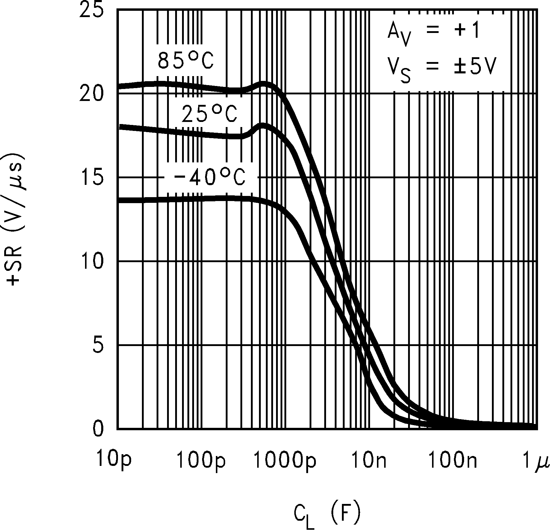
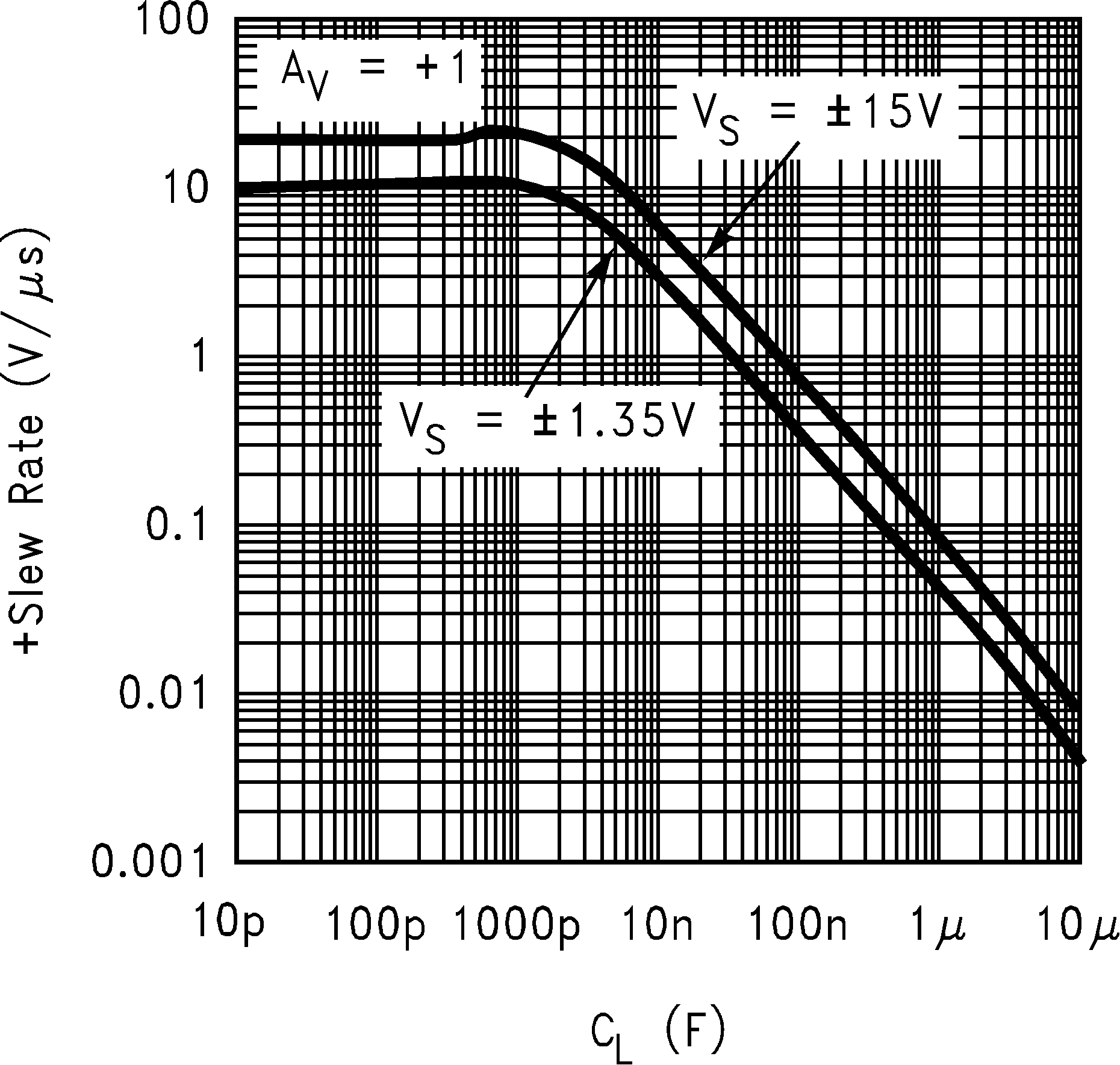
| SR | Slew Rate(8) | AV = +1,VI = 2 VPP | 9 | V/µs | |||
| fu | Unity Gain-Frequency | VI = 10 mV, RL = 2 KΩ to V+/2 | 10 | MHz | |||
| GBWP | Gain Bandwidth Product | f = 50 KHz | 21 | 15.5 | MHz | ||
| −65°C ≤ TJ ≤ +150°C | 14 | ||||||
| Phim | Phase Margin | VI = 10 mV | 50 | Deg | |||
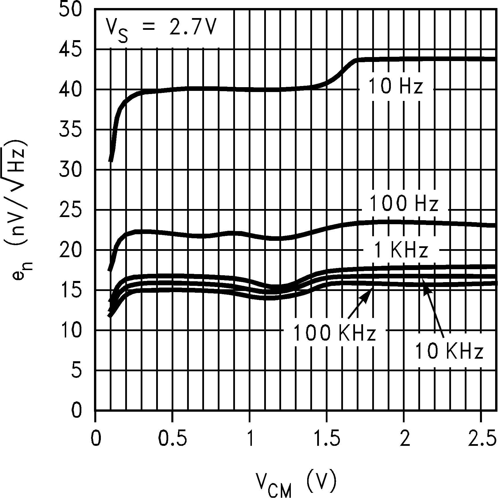
| en | Input-Referred Voltage Noise | f = 2 KHz, RS = 50 Ω | 15 | nV/ √Hz | |||
| in | Input-Referred Current Noise | f = 2 KHz | 1 | pA/ √Hz | |||
| fMAX | Full Power Bandwidth | ZL = (20 pF || 10 KΩ) to V+/2 | 1 | MHz | |||
(1) Electrical Table values apply only for factory testing conditions at the temperature indicated. Factory testing conditions result in very limited self-heating of the device such that TJ = TA. No guarantee of parametric performance is indicated in the electrical tables under conditions of internal self heating where TJ > TA.
(2) Typical Values represent the most likely parametric norm.
(3) All limits are guaranteed by testing or statistical analysis.
(4) Offset voltage average drift determined by dividing the change in VOS at temperature extremes into the total temperature change.
(5) Positive current corresponds to current flowing into the device.
(6) Production Short Circuit test is a momentary test. See Note 7.
(7) Allowable Output Short Circuit duration is infinite for VS ≤ 6V at room temperature and below. For VS > 6V, allowable short circuit duration is 1.5 ms.
(8) Slew rate is the slower of the rising and falling slew rates. Connected as a Voltage Follower.
6.6 Electrical Characteristics 5 V(1)
Unless otherwise specified, all limited guaranteed for TA = 25°C, V+ = 5 V, V− = 0 V, VCM = 1 V, VO = V+/2, and RL > 1 MΩ to V−.| PARAMETER | TEST CONDITIONS | MIN | TYP(2) | MAX(3) | UNIT | ||
|---|---|---|---|---|---|---|---|
| VOS | Input Offset Voltage | VCM = 1 V & VCM = 4.5 V | +/−0.7 | +/−5 | mV | ||
| −65°C ≤ TJ ≤ +150°C | +/− 7 | ||||||
| TC VOS | Input Offset Average Drift | VCM = 1 V & VCM = 4.5 V(4) | +/−2 | µV/°C | |||
| IB | Input Bias Current | VCM = 1 V(5) | −1.18 | −2.00 | µA | ||
| −65°C ≤ TJ ≤ +150°C | −2.70 | ||||||
| VCM = 4.5 V(5) | +0.49 | +1.00 | |||||
| −65°C ≤ TJ ≤ +150°C | +1.60 | ||||||
| IOS | Input Offset Current | VCM = 1 V & VCM = 4.5 V | 20 | 250 | nA | ||
| −65°C ≤ TJ ≤ +150°C | 400 | ||||||
| CMRR | Common Mode Rejection Ratio | VCM stepped from 0 V to 3.3 V |
110 | 84 | dB | ||
| −65°C ≤ TJ ≤ +150°C | 72 | ||||||
| VCM stepped from 4 V to 5 V |
100 | ||||||
| VCM stepped from 0 V to 5 V |
80 | 64 | |||||
| −65°C ≤ TJ ≤ +150°C | 61 | ||||||
| +PSRR | Positive Power Supply Rejection Ratio | V+ = 2.7 V to 5 V, VCM = 0.5 V |
104 | 78 | dB | ||
| −65°C ≤ TJ ≤ +150°C | 74 | ||||||
| CMVR | Input Common-Mode Voltage Range | CMRR > 50 dB | −0.3 | −0.1 | V | ||
| −65°C ≤ TJ ≤ +150°C | 0.0 | ||||||
| 5.3 | 5.1 | V | |||||
| −65°C ≤ TJ ≤ +150°C | 5.0 | ||||||
| AVOL | Large Signal Voltage Gain | VO = 0.5 to 4.5 V, RL = 10 K to V− |
84 | 74 | dB | ||
| −65°C ≤ TJ ≤ +150°C | 70 | ||||||
| VO = 0.5 to 4.5 V, RL = 2 K to V− |
80 | 70 | |||||
| −65°C ≤ TJ ≤ +150°C | 66 | ||||||
| VO | Output Swing High | RL = 10 K to V− | 4.87 | 4.75 | V | ||
| −65°C ≤ TJ ≤ +150°C | 4.72 | ||||||
| RL = 2 K to V− | 4.81 | 4.70 | |||||
| −65°C ≤ TJ ≤ +150°C | 4.66 | ||||||
| Output Swing Low | RL = 10 K to V− | 86 | 125 | mV | |||
| −65°C ≤ TJ ≤ +150°C | 135 | ||||||
| ISC | Output Short Circuit Current | Sourcing to V−
VID = 200 mV(6)(7) |
53 | 35 | mA | ||
| −65°C ≤ TJ ≤ +150°C | 20 | ||||||
| Sinking to V+
VID = −200 mV(6)(7) |
75 | 60 | |||||
| −65°C ≤ TJ ≤ +150°C | 50 | ||||||
| IS | Supply Current | No load, VCM = 1 V | 0.97 | 1.25 | mA | ||
| −65°C ≤ TJ ≤ +150°C | 1.75 | ||||||
| SR | Slew Rate(8) | AV = +1, VI = 5 VPP | 12 | 10 | V/µs | ||
| −65°C ≤ TJ ≤ +150°C | 7 | ||||||
| fu | Unity Gain Frequency | VI = 10 mV, RL = 2 KΩ to V+/2 |
10.5 | MHz | |||
| GBWP | Gain-Bandwidth Product | f = 50 KHz | 21 | 16 | MHz | ||
| −65°C ≤ TJ ≤ +150°C | 15 | ||||||
| Phim | Phase Margin | VI = 10 mV | 53 | Deg | |||
| en | Input-Referred Voltage Noise | f = 2 KHz, RS = 50 Ω | 15 | nV/ √hZ | |||
| in | Input-Referred Current Noise | f = 2 KHz | 1 | pA/ √hZ | |||
| fMAX | Full Power Bandwidth | ZL = (20 pF || 10 kΩ) to V+/2 | 900 | KHz | |||
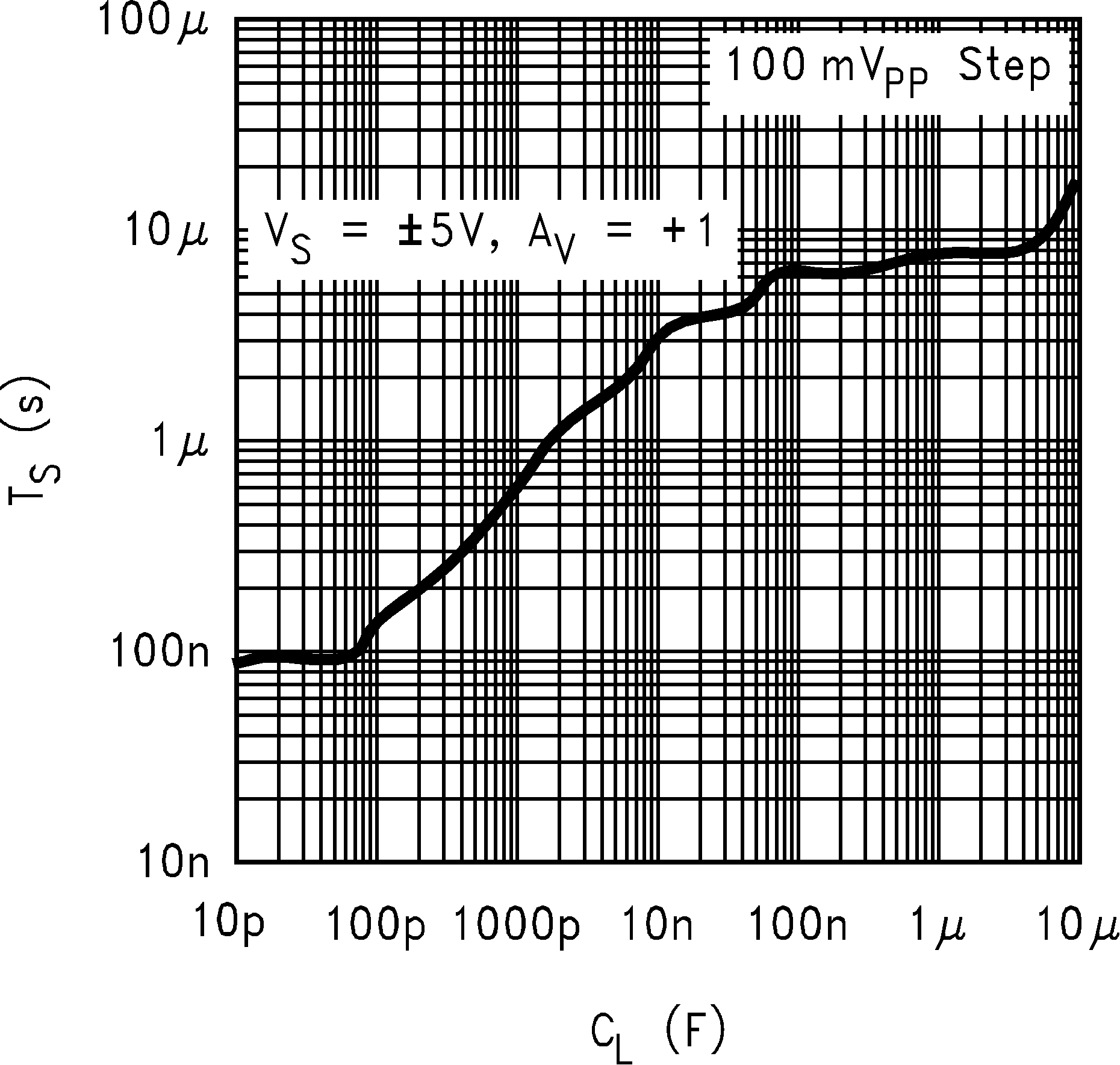
| tS | Settling Time (±5%) | 100 mVPP Step, 500 pF load | 400 | ns | |||
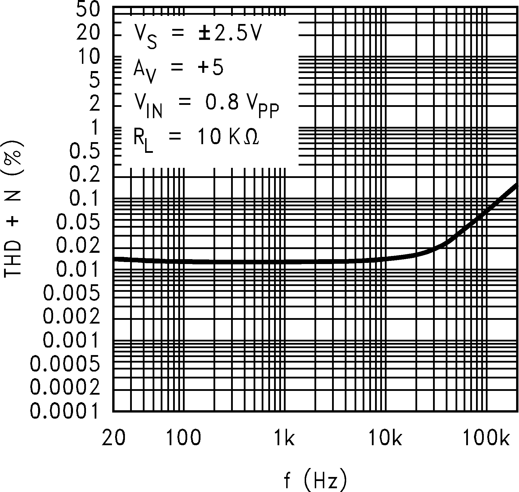
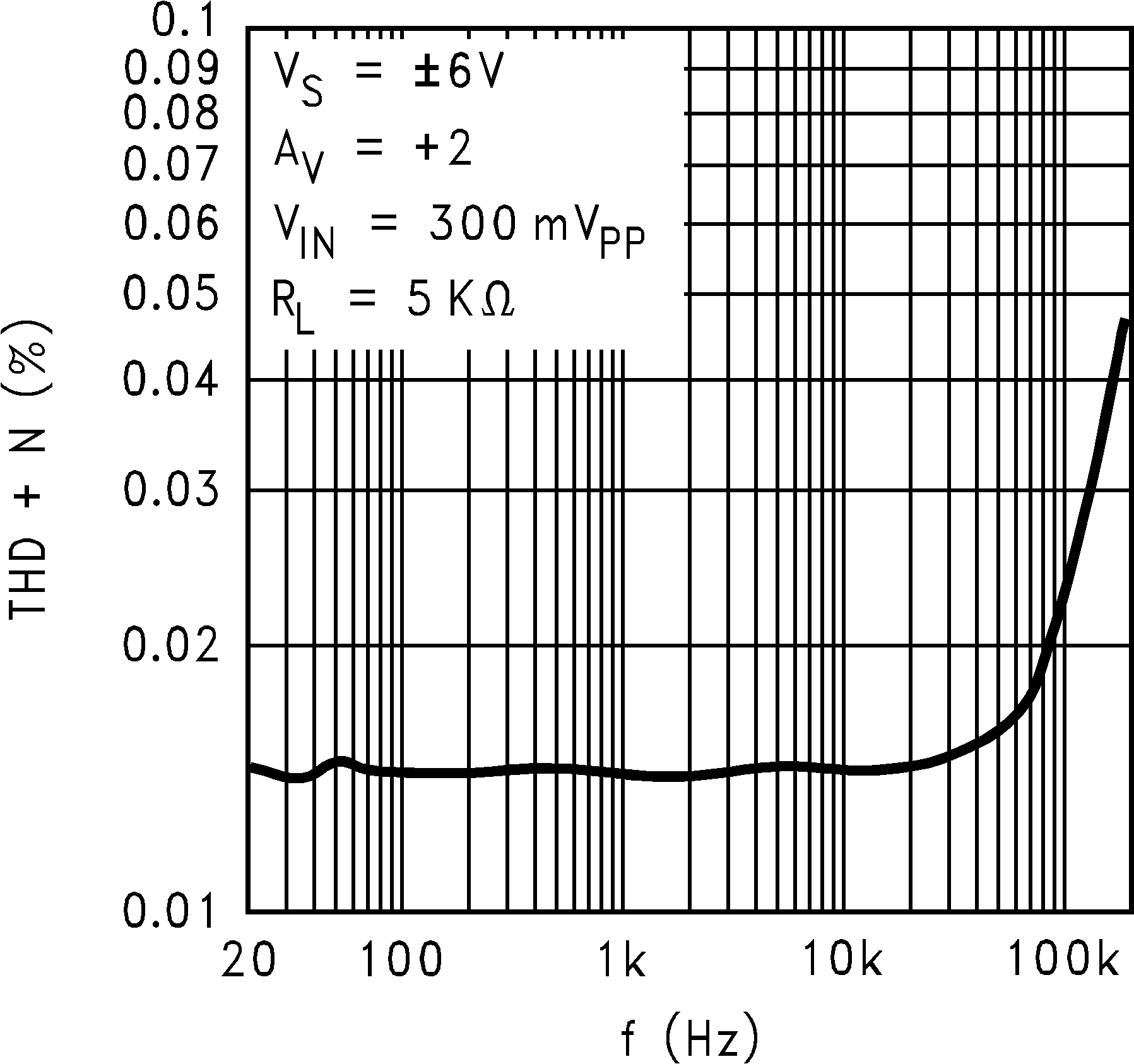
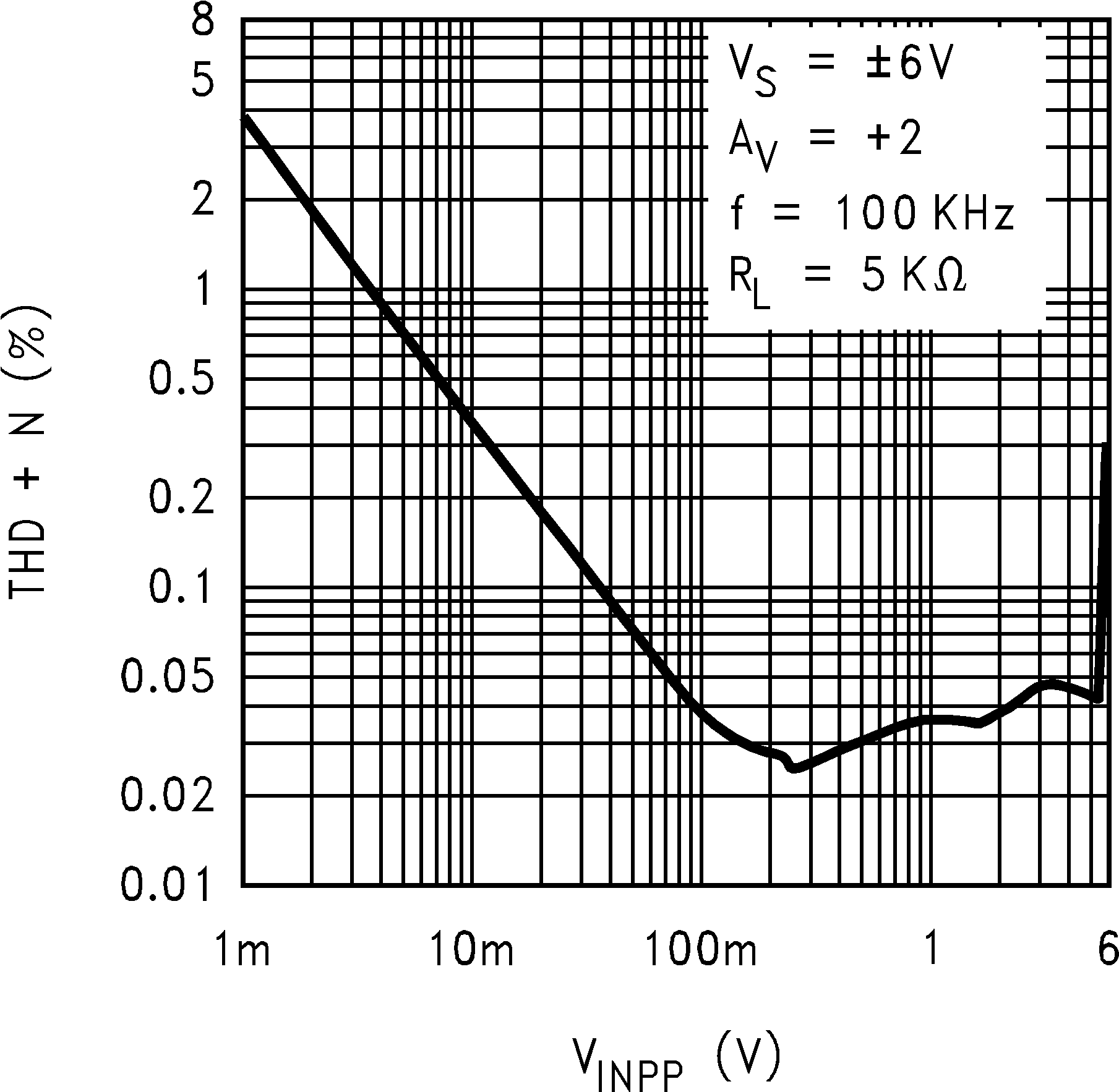
| THD+N | Total Harmonic Distortion + Noise | RL = 1 KΩ to V+/2 f = 10 KHz to AV= +2, 4 VPP swing |
0.05% | ||||
(1) Electrical Table values apply only for factory testing conditions at the temperature indicated. Factory testing conditions result in very limited self-heating of the device such that TJ = TA. No guarantee of parametric performance is indicated in the electrical tables under conditions of internal self heating where TJ > TA.
(2) Typical Values represent the most likely parametric norm.
(3) All limits are guaranteed by testing or statistical analysis.
(4) Offset voltage average drift determined by dividing the change in VOS at temperature extremes into the total temperature change.
(5) Positive current corresponds to current flowing into the device.
(6) Production Short Circuit test is a momentary test. See Note 7.
(7) Allowable Output Short Circuit duration is infinite for VS ≤ 6V at room temperature and below. For VS > 6V, allowable short circuit duration is 1.5ms.
(8) Slew rate is the slower of the rising and falling slew rates. Connected as a Voltage Follower.
6.7 Electrical Characteristics ±15 V(7)
Unless otherwise specified, all limited guaranteed for TA = 25°C, V+ = 15 V, V− = −15 V, VCM = 0 V, VO = 0 V, and RL > 1 MΩ to 0 V.| PARAMETER | TEST CONDITIONS | MIN | TYP(1) | MAX(2) | UNIT | ||
|---|---|---|---|---|---|---|---|
| VOS | Input Offset Voltage | VCM = −14.5 V & VCM = 14.5 V | +/−0.7 | +/−7 | mV | ||
| −65°C ≤ TJ ≤ +150°C | +/− 9 | ||||||
| TC VOS | Input Offset Average Drift | VCM = −14.5 V & VCM = 14.5 V(6) | +/−2 | µV/°C | |||
| IB | Input Bias Current | VCM = −14.5 V(3) | −1.05 | −2.00 | µA | ||
| −65°C ≤ TJ ≤ +150°C | −2.80 | ||||||
| VCM = 14.5 V(3) | +0.49 | +1.00 | |||||
| −65°C ≤ TJ ≤ +150°C | +1.50 | ||||||
| IOS | Input Offset Current | VCM = −14.5 V & VCM = 14.5 V | 30 | 275 | nA | ||
| −65°C ≤ TJ ≤ +150°C | 550 | ||||||
| CMRR | Common Mode Rejection Ratio | VCM stepped from −15 V to 13 V | 100 | 84 | dB | ||
| −65°C ≤ TJ ≤ +150°C | 80 | ||||||
| VCM stepped from 14 V to 15 V | 100 | ||||||
| VCM stepped from −15 V to 15 V | 88 | 74 | |||||
| −65°C ≤ TJ ≤ +150°C | 72 | ||||||
| +PSRR | Positive Power Supply Rejection Ratio | V+ = 12 V to 15 V | 100 | 70 | dB | ||
| −65°C ≤ TJ ≤ +150°C | 66 | ||||||
| −PSRR | Negative Power Supply Rejection Ratio | V− = −12 V to −15 V | 100 | 70 | dB | ||
| −65°C ≤ TJ ≤ +150°C | 66 | ||||||
| CMVR | Input Common-Mode Voltage Range | CMRR > 50 dB | −15.3 | −15.1 | V | ||
| −65°C ≤ TJ ≤ +150°C | −15.0 | ||||||
| 15.3 | 15.1 | V | |||||
| −65°C ≤ TJ ≤ +150°C | 15.0 | ||||||
| AVOL | Large Signal Voltage Gain | VO = 0 V to ±13 V, RL = 10 KΩ |
85 | 78 | dB | ||
| −65°C ≤ TJ ≤ +150°C | 74 | ||||||
| VO = 0 V to ±13 V, RL = 2 KΩ |
79 | 72 | |||||
| −65°C ≤ TJ ≤ +150°C | 66 | ||||||
| VO | Output Swing High | RL = 10 KΩ | 14.83 | 14.65 | V | ||
| −65°C ≤ TJ ≤ +150°C | 14.61 | ||||||
| RL = 2 KΩ | 14.73 | 14.60 | |||||
| −65°C ≤ TJ ≤ +150°C | 14.55 | ||||||
| Output Swing Low | RL = 10 KΩ | −14.91 | −14.75 | V | |||
| −65°C ≤ TJ ≤ +150°C | −14.65 | ||||||
| RL = 2 KΩ | −14.83 | −14.65 | |||||
| −65°C ≤ TJ ≤ +150°C | −14.60 | ||||||
| ISC | Output Short Circuit Current | Sourcing to ground VID = 200 mV(5)(5) |
60 | 40 | mA | ||
| −65°C ≤ TJ ≤ +150°C | 25 | ||||||
| Sinking to ground VID = 200 mV(5)(5) |
100 | 70 | |||||
| −65°C ≤ TJ ≤ +150°C | 60 | ||||||
| IS | Supply Current | No load, VCM = 0 V | 1.30 | 1.50 | mA | ||
| −65°C ≤ TJ ≤ +150°C | 1.90 | ||||||
| SR | Slew Rate(4) | AV = +1, VI = 24 VPP | 15 | 10 | V/µs | ||
| −65°C ≤ TJ ≤ +150°C | 8 | ||||||
| fu | Unity Gain Frequency | VI = 10 mV, RL = 2 KΩ | 14 | MHz | |||
| GBWP | Gain-Bandwidth Product | f = 50 KHz | 24 | 18 | MHz | ||
| −65°C ≤ TJ ≤ +150°C | 16 | ||||||
| Phim | Phase Margin | VI = 10 mV | 58 | Deg | |||
| en | Input-Referred Voltage Noise | f = 2 KHz, RS = 50 Ω | 15 | nV/ √hZ | |||
| in | Input-Referred Current Noise | f = 2 KHz | 1 | pA/ √hZ | |||
| fMAX | Full Power Bandwidth | ZL = 20 pF || 10 KΩ | 160 | KHz | |||
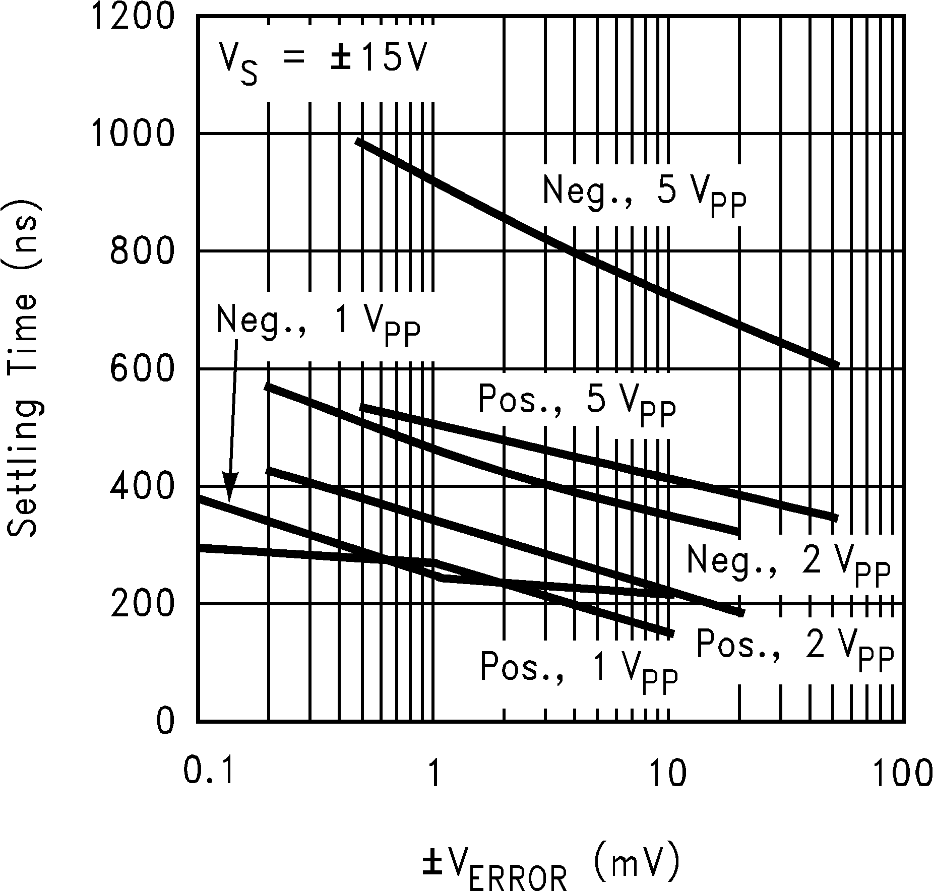
| ts | Settling Time (±1%, AV = +1) | Positive Step, 5 VPP | 320 | ns | |||
| Negative Step, 5 VPP | 600 | ||||||
| THD+N | Total Harmonic Distortion +Noise | RL = 1 KΩ, f = 10 KHz, AV = +2, 28VPP swing |
0.01% | ||||
(1) Typical Values represent the most likely parametric norm.
(2) All limits are guaranteed by testing or statistical analysis.
(3) Positive current corresponds to current flowing into the device.
(4) Slew rate is the slower of the rising and falling slew rates. Connected as a Voltage Follower.
(5) Production Short Circuit test is a momentary test. See Note 7.
(6) Offset voltage average drift determined by dividing the change in VOS at temperature extremes into the total temperature change.
(7) Electrical Table values apply only for factory testing conditions at the temperature indicated. Factory testing conditions result in very limited self-heating of the device such that TJ = TA. No guarantee of parametric performance is indicated in the electrical tables under conditions of internal self heating where TJ > TA.
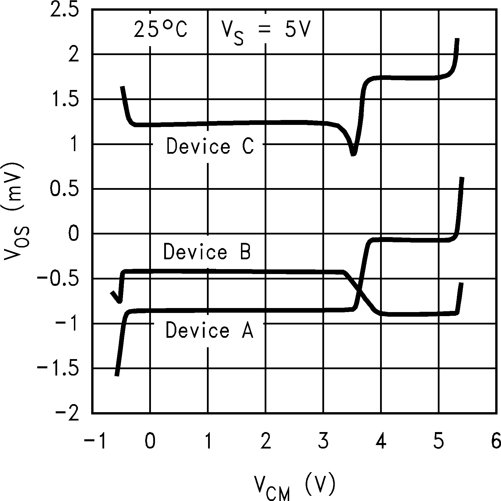
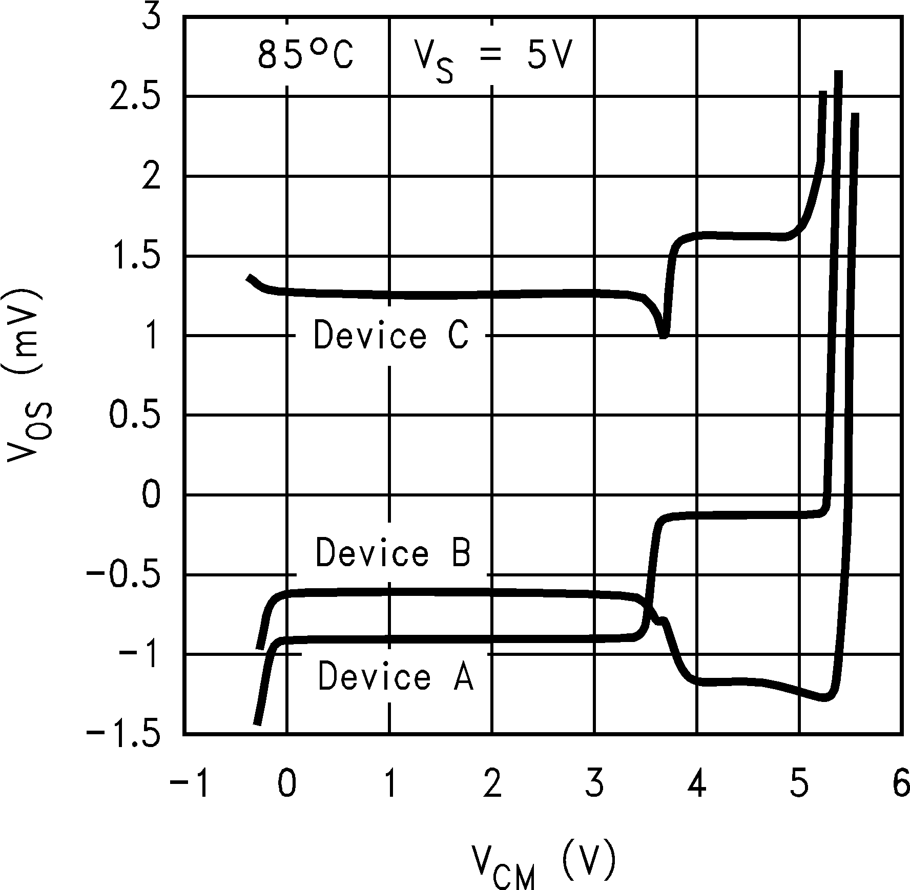
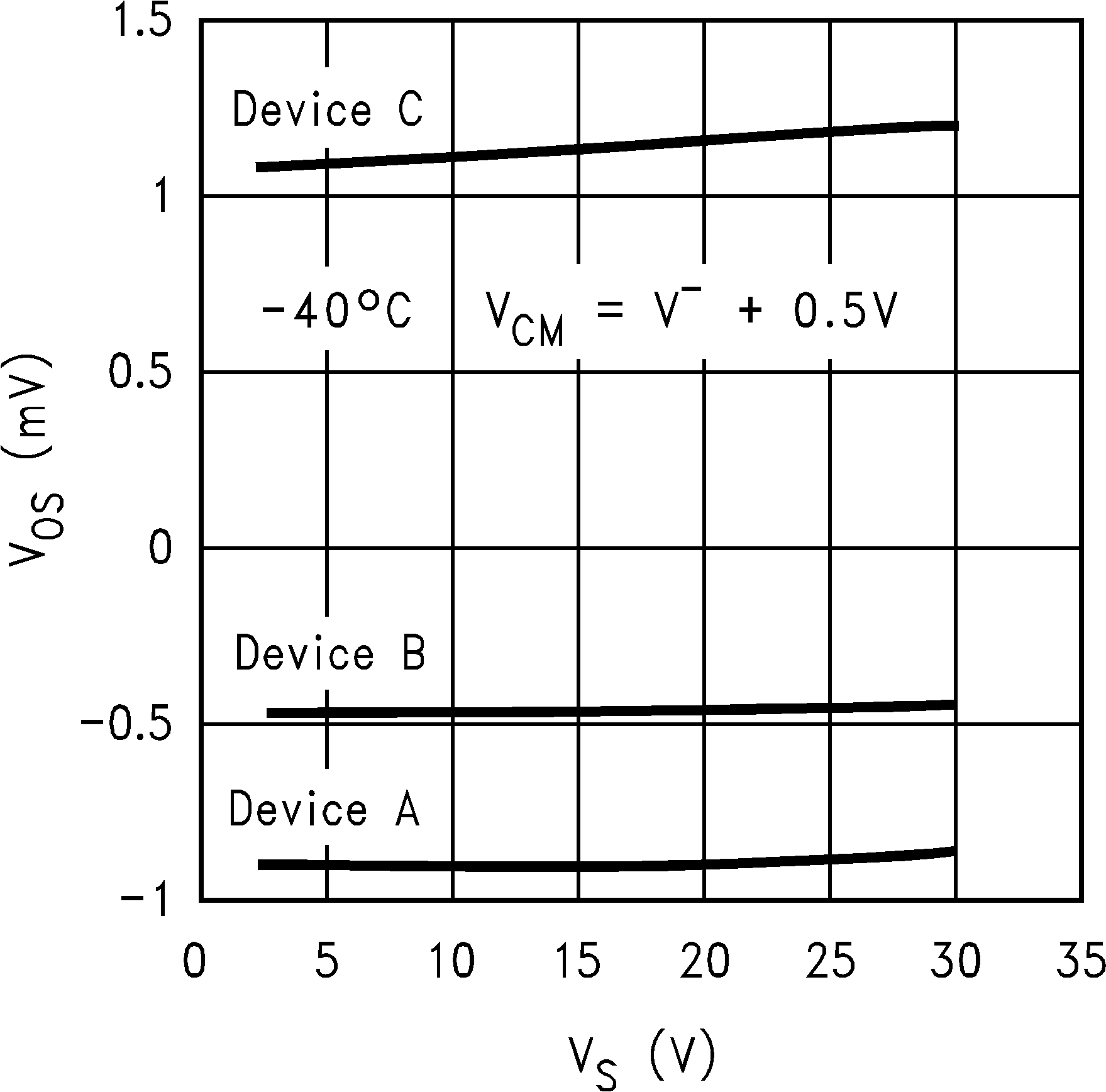
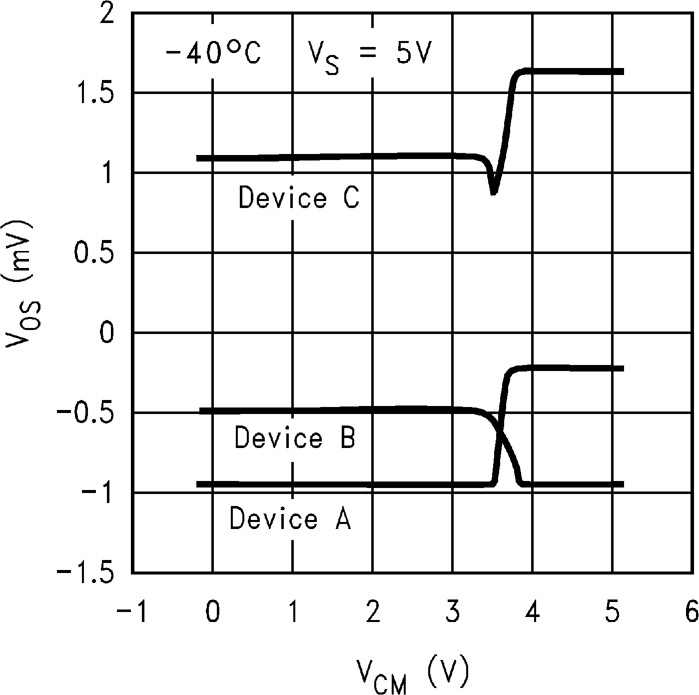
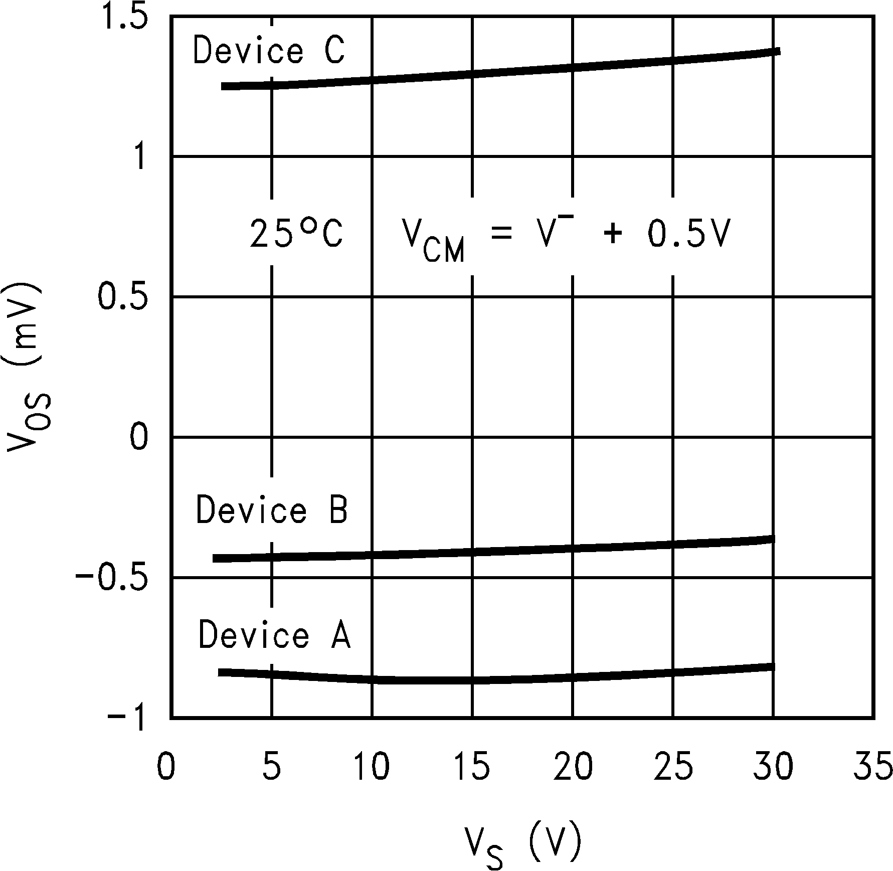
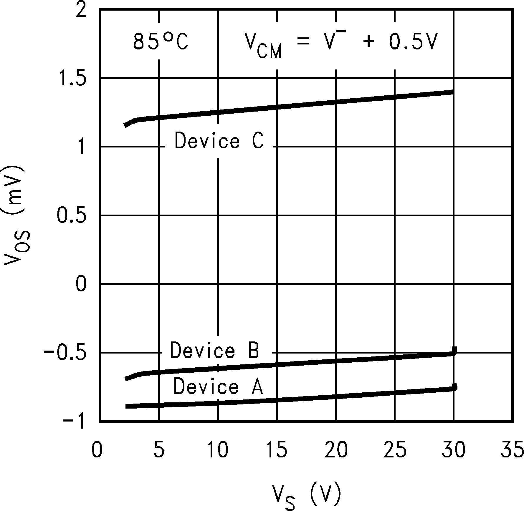
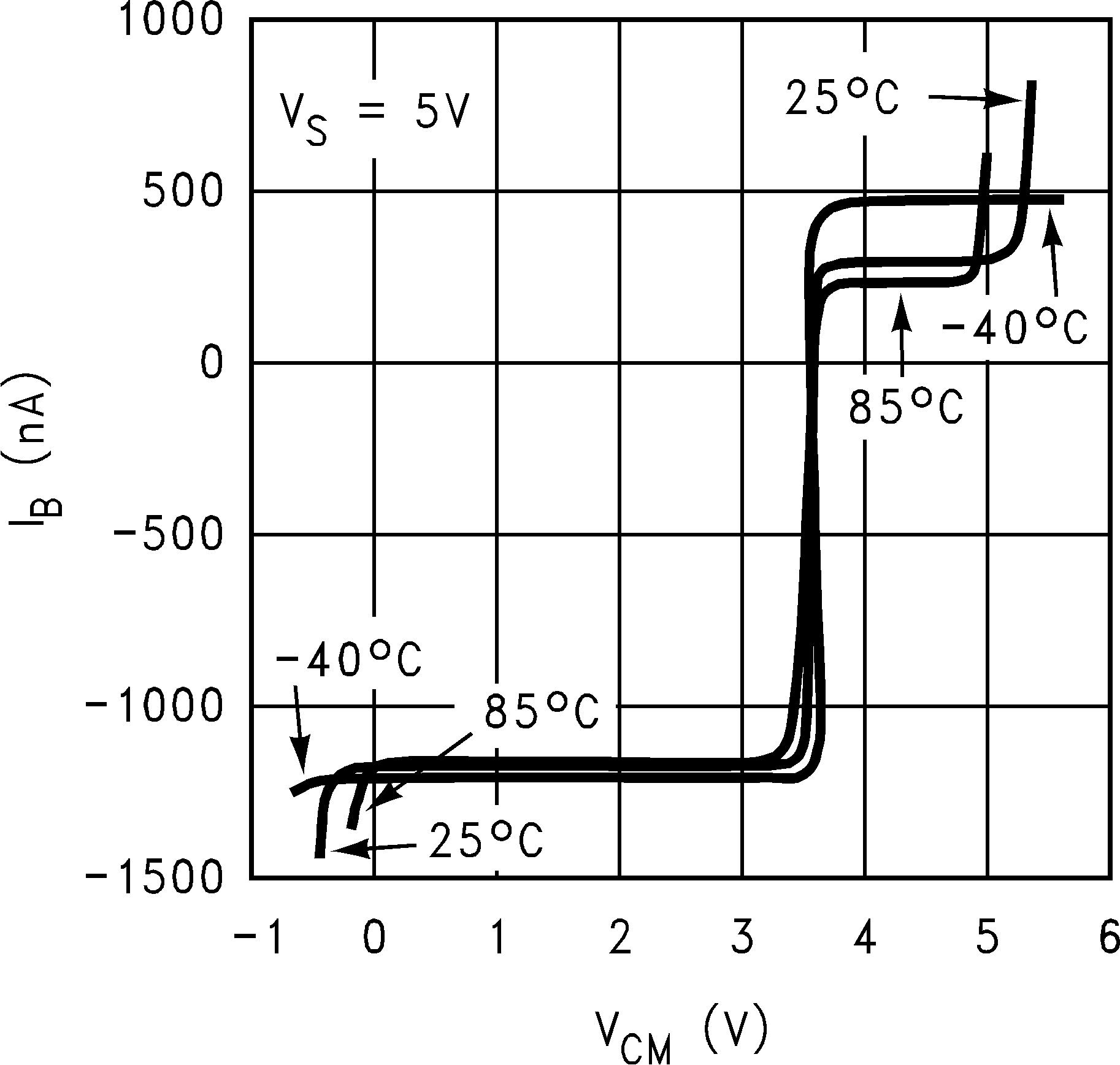
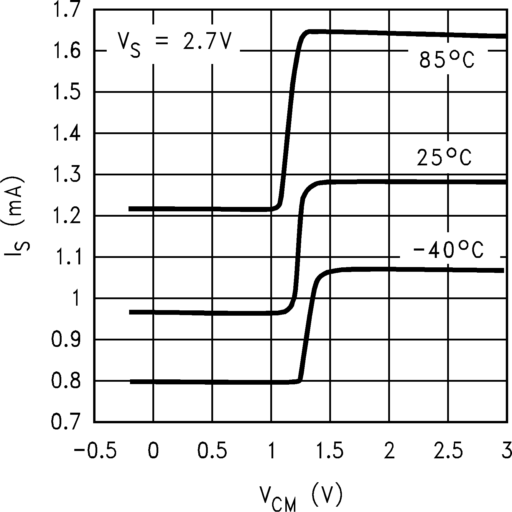
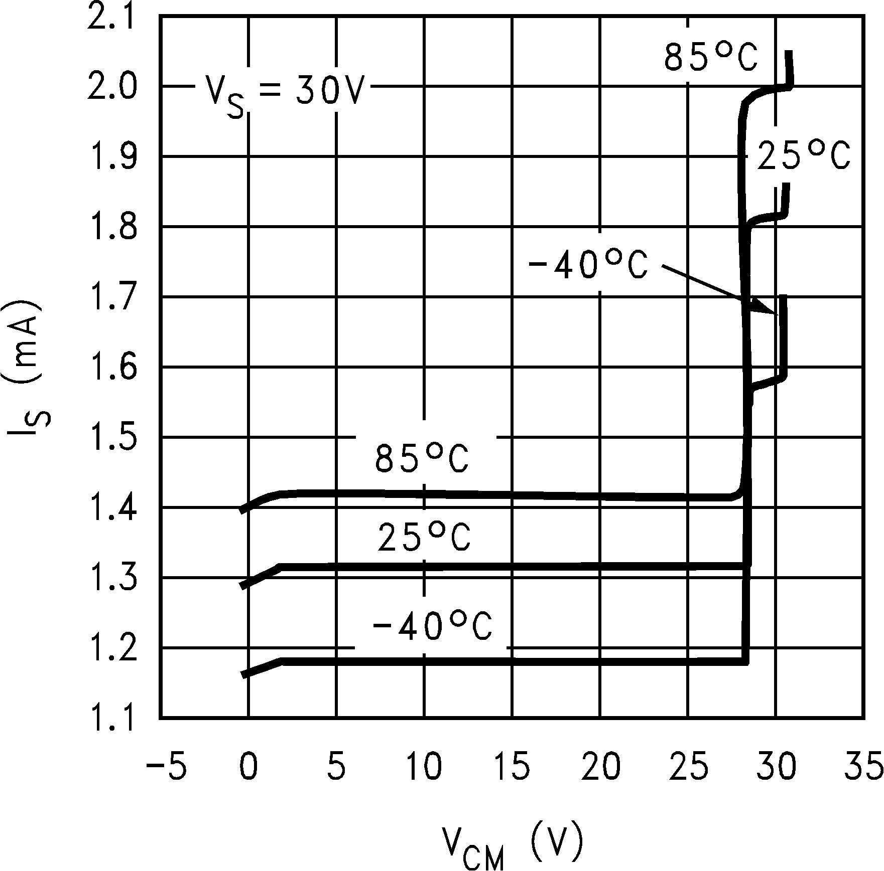
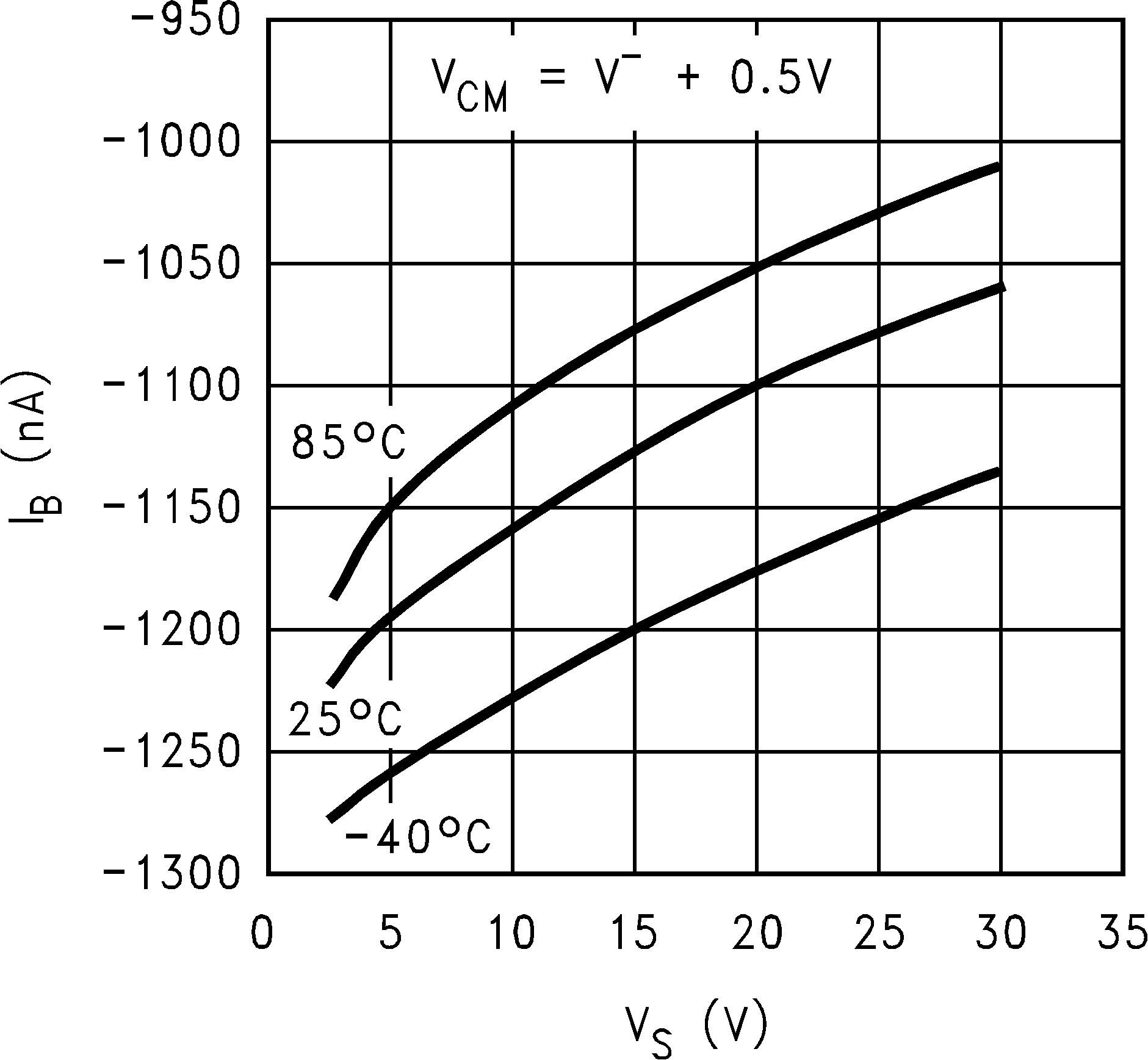
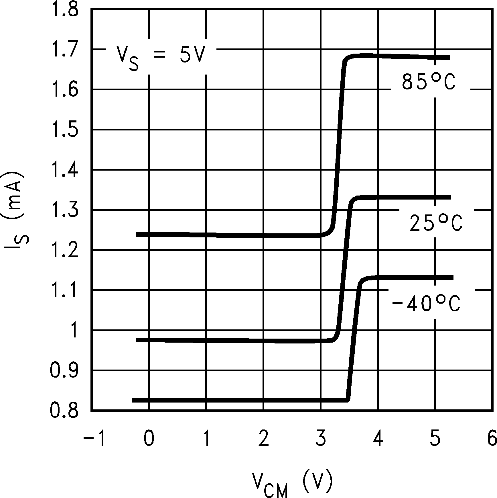
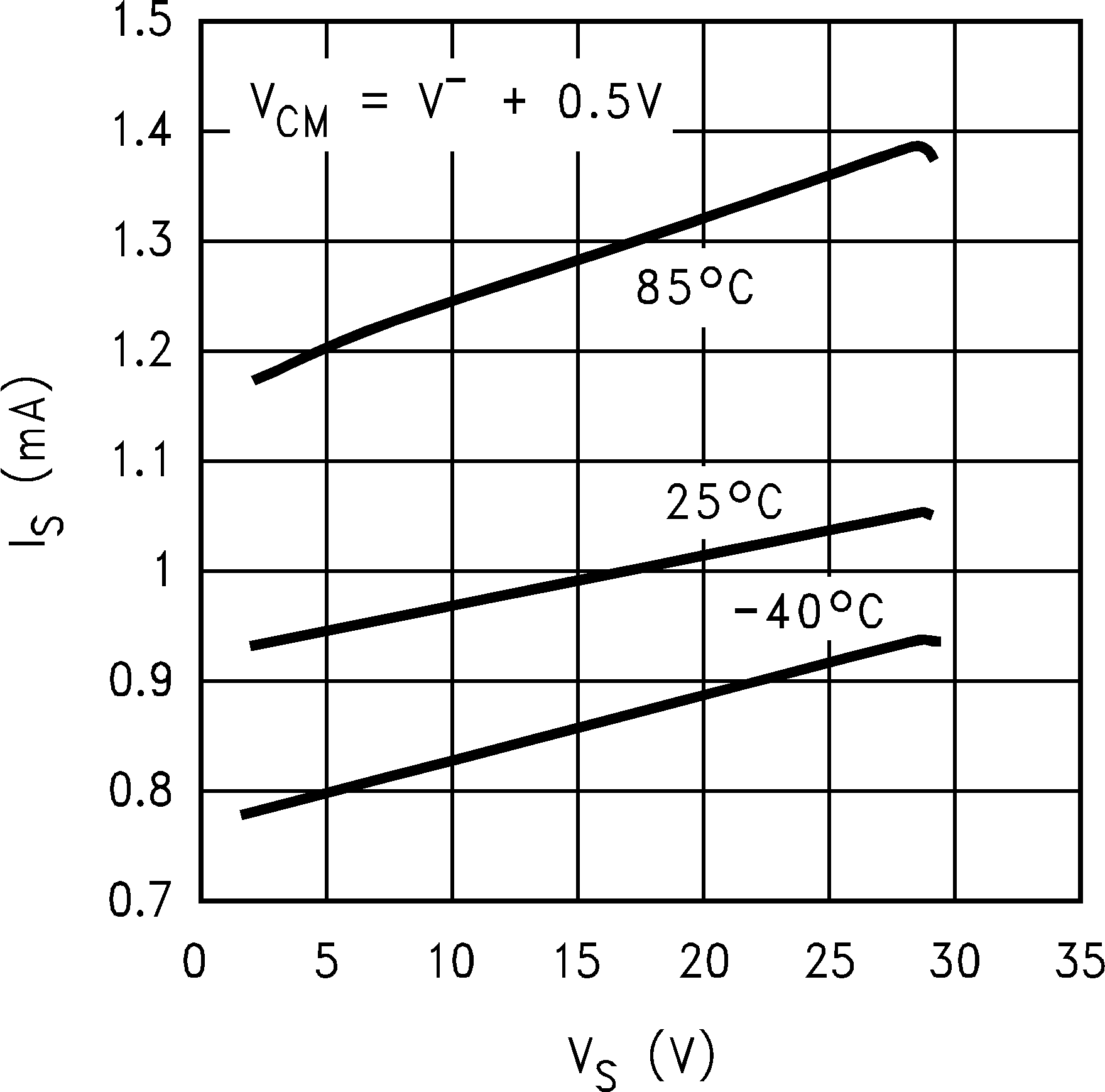
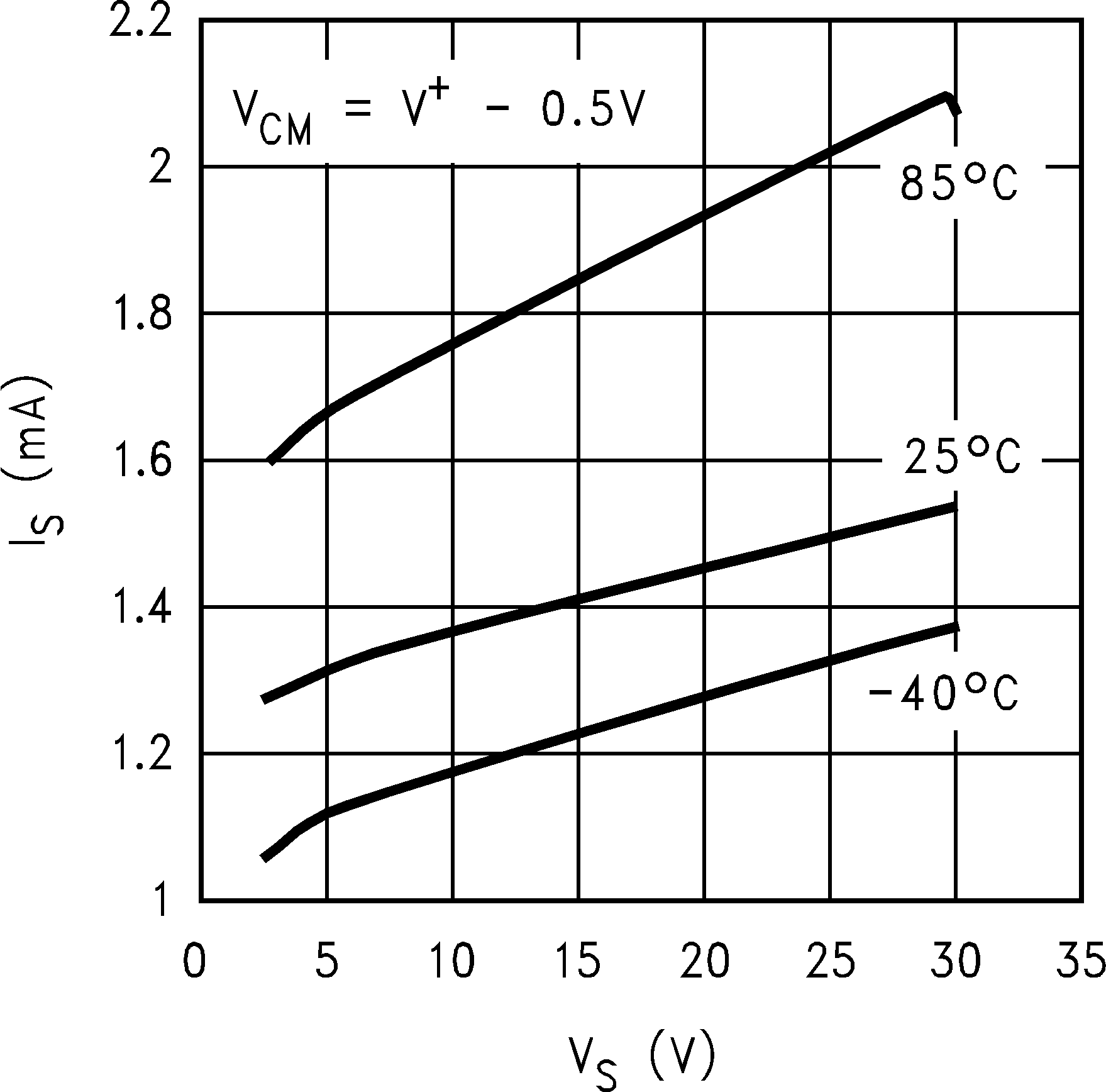
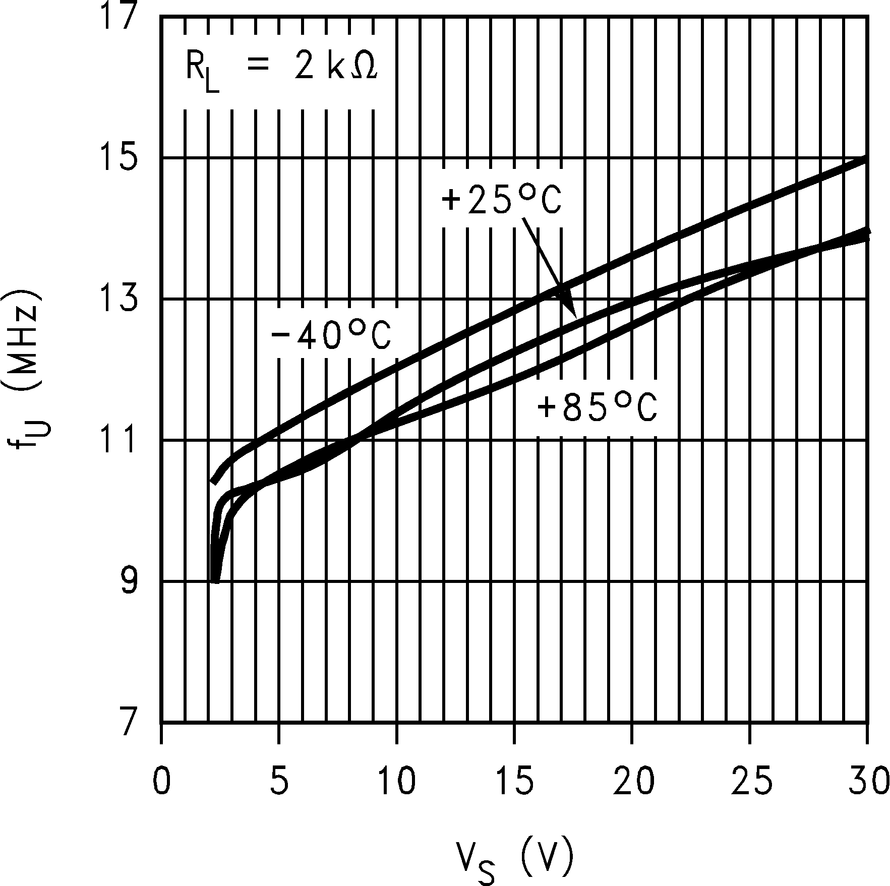
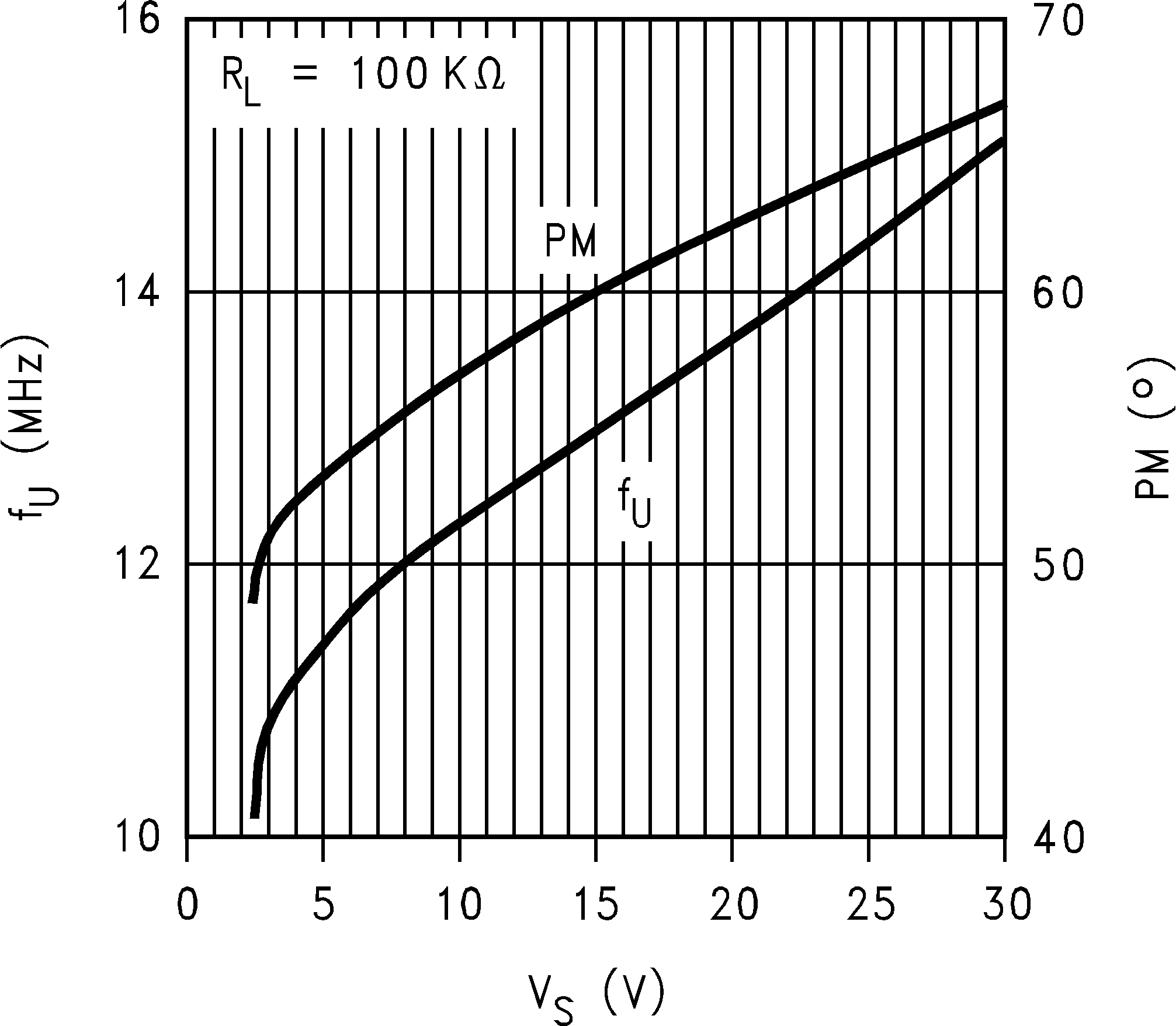
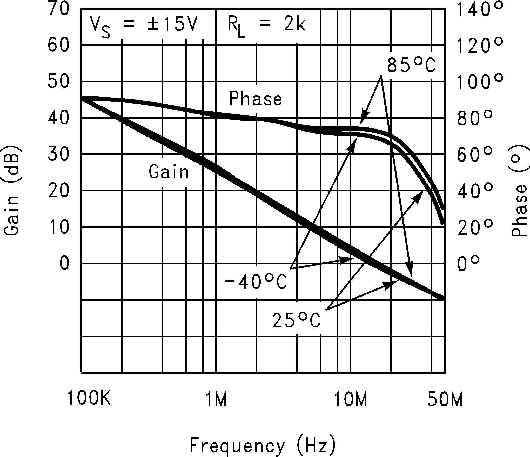
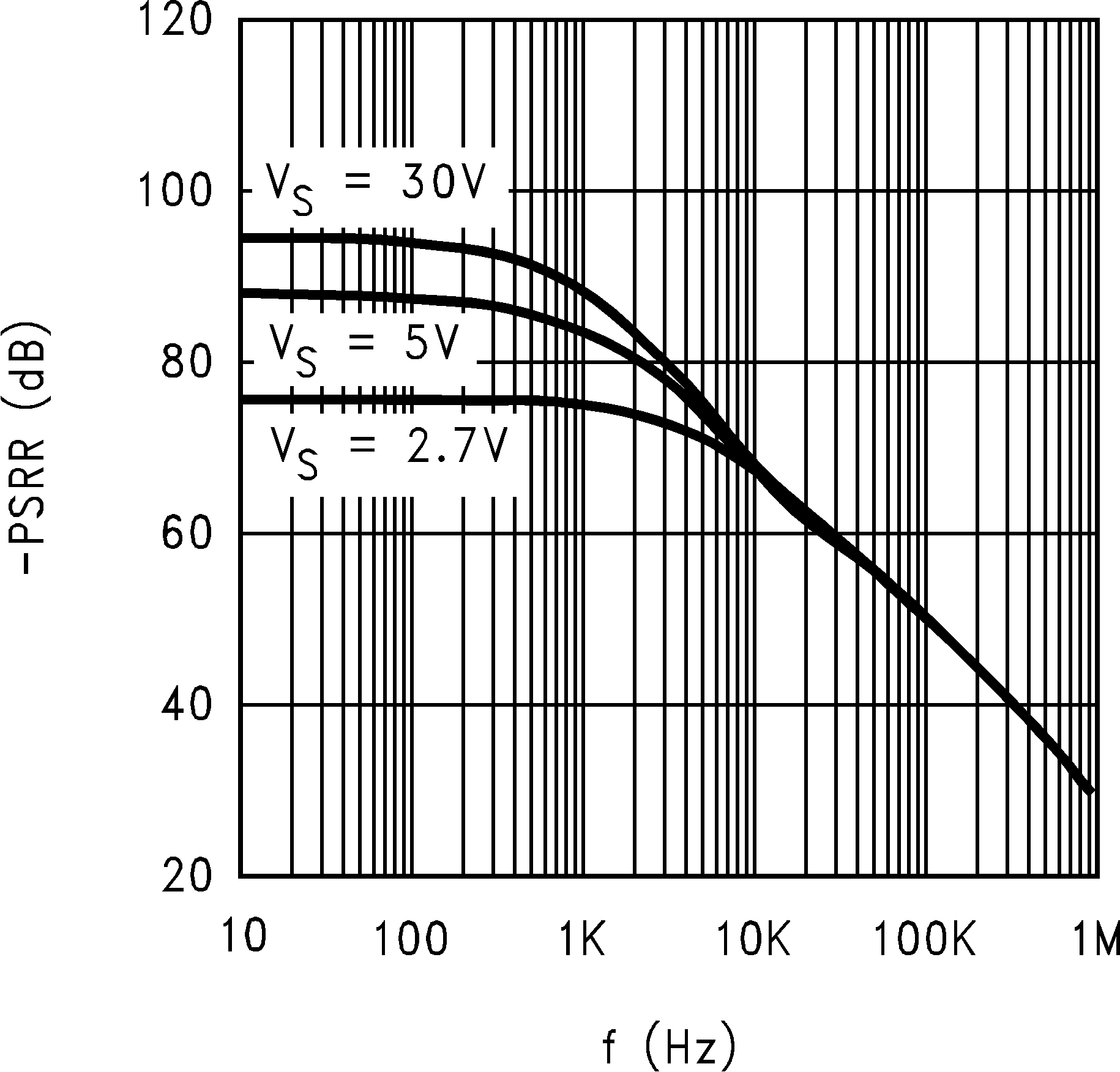
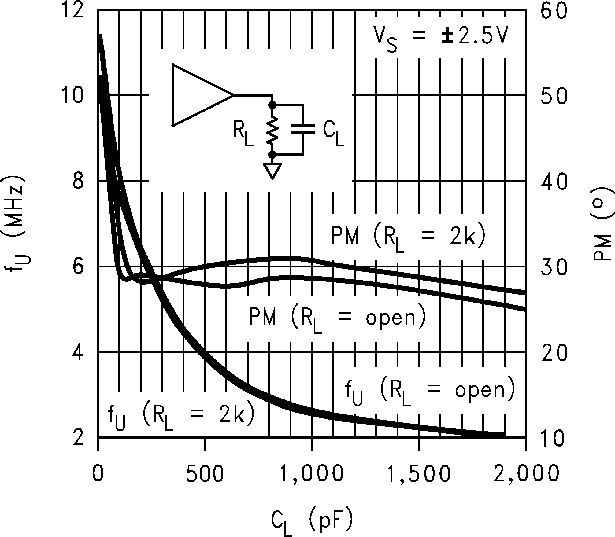
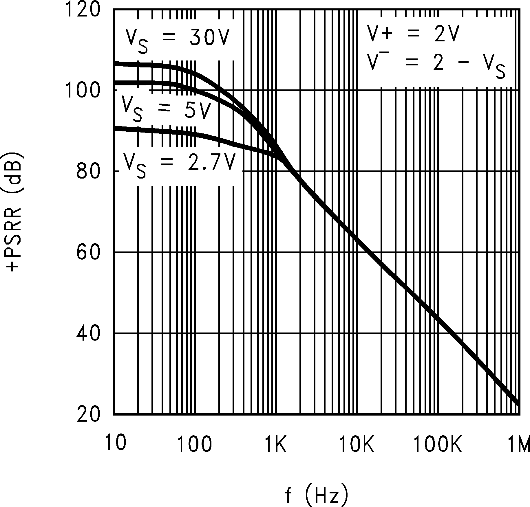
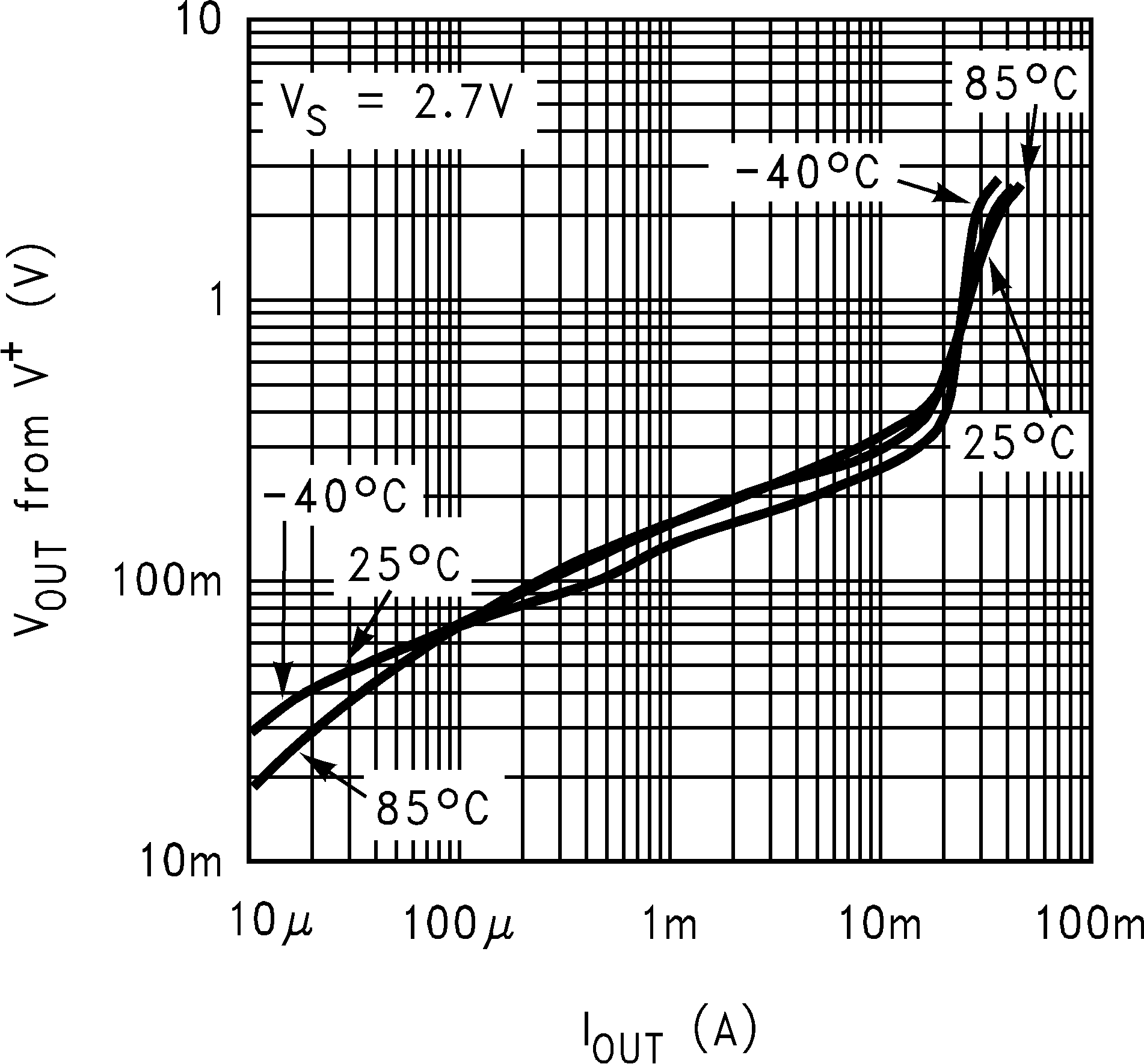
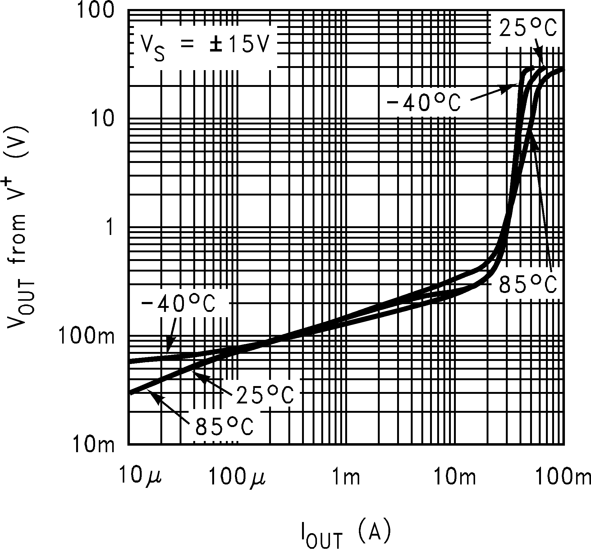
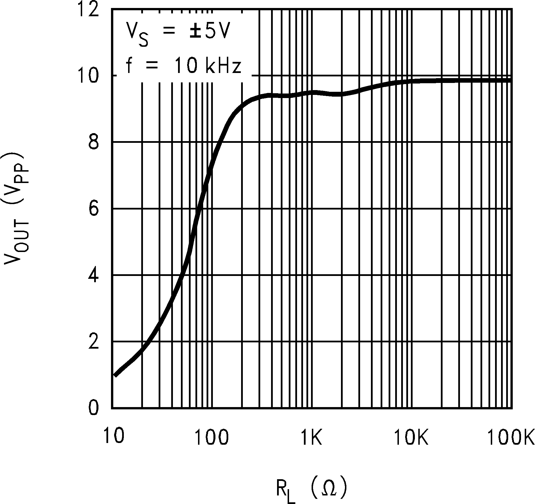
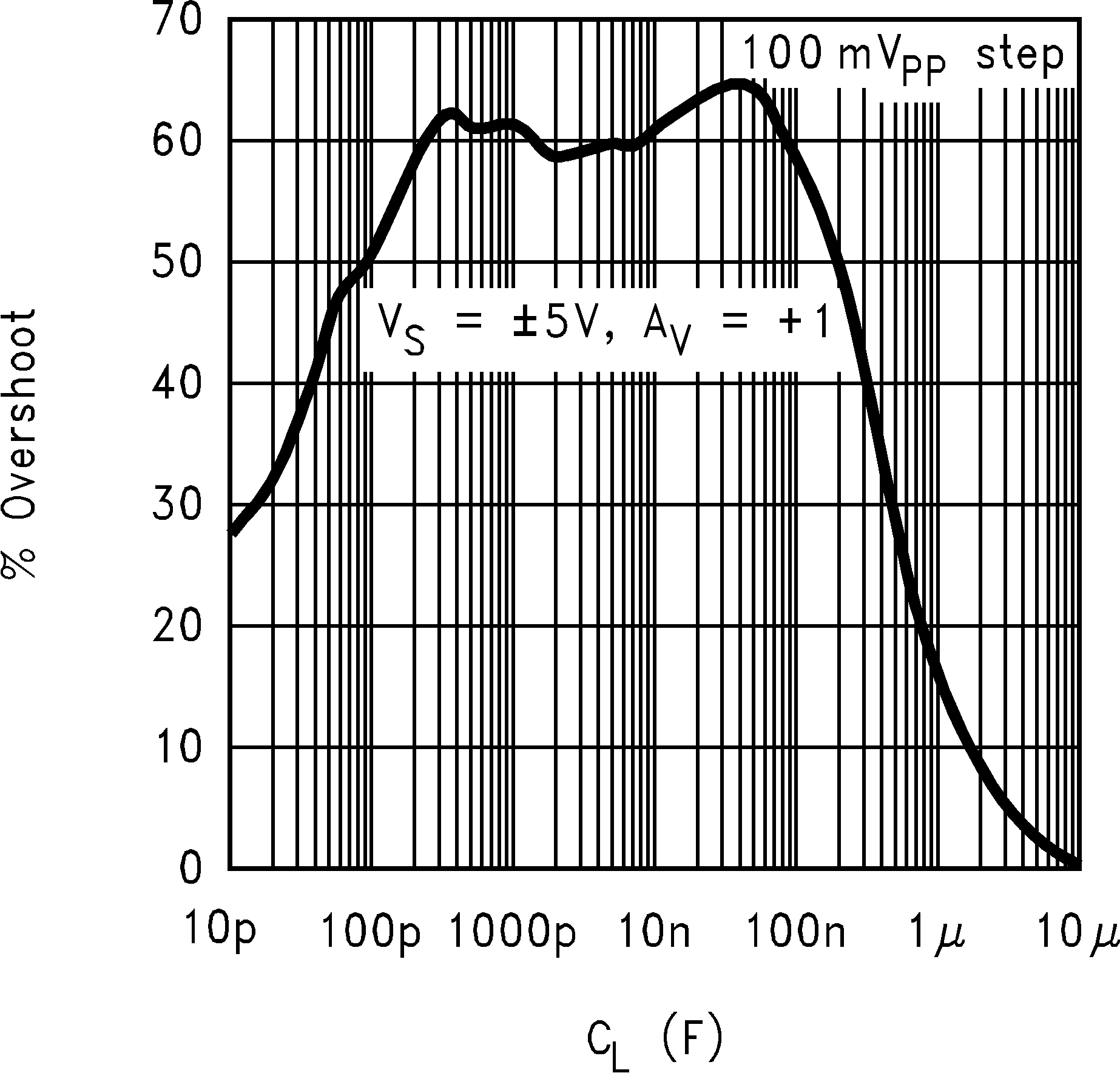
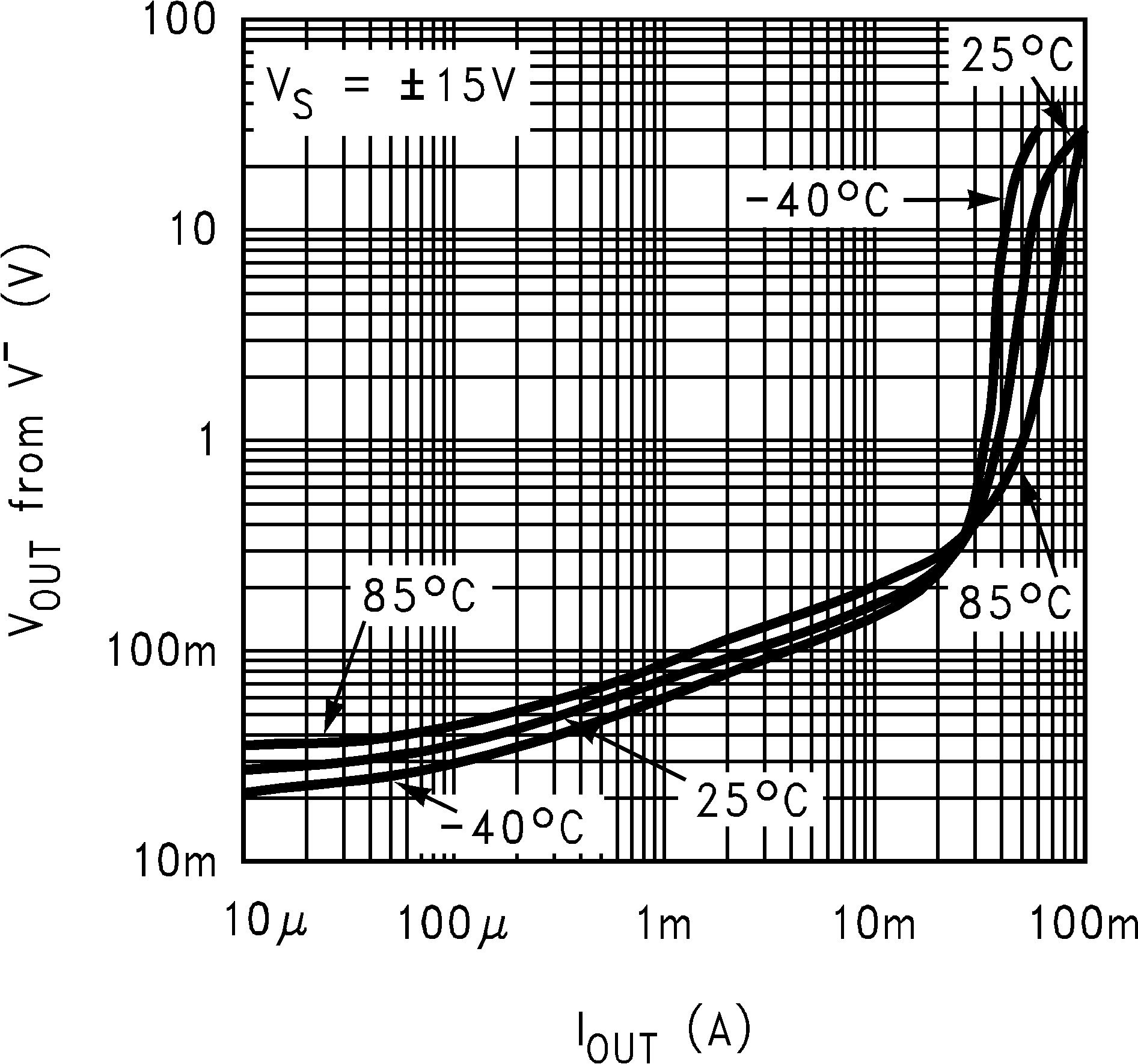
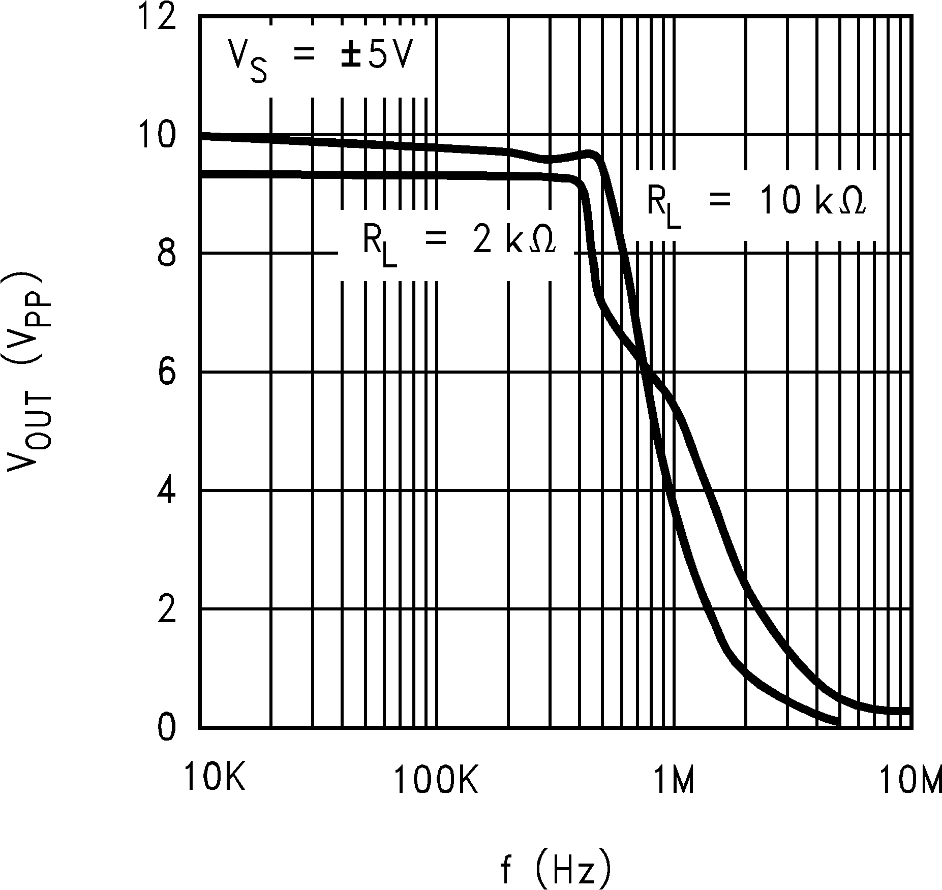
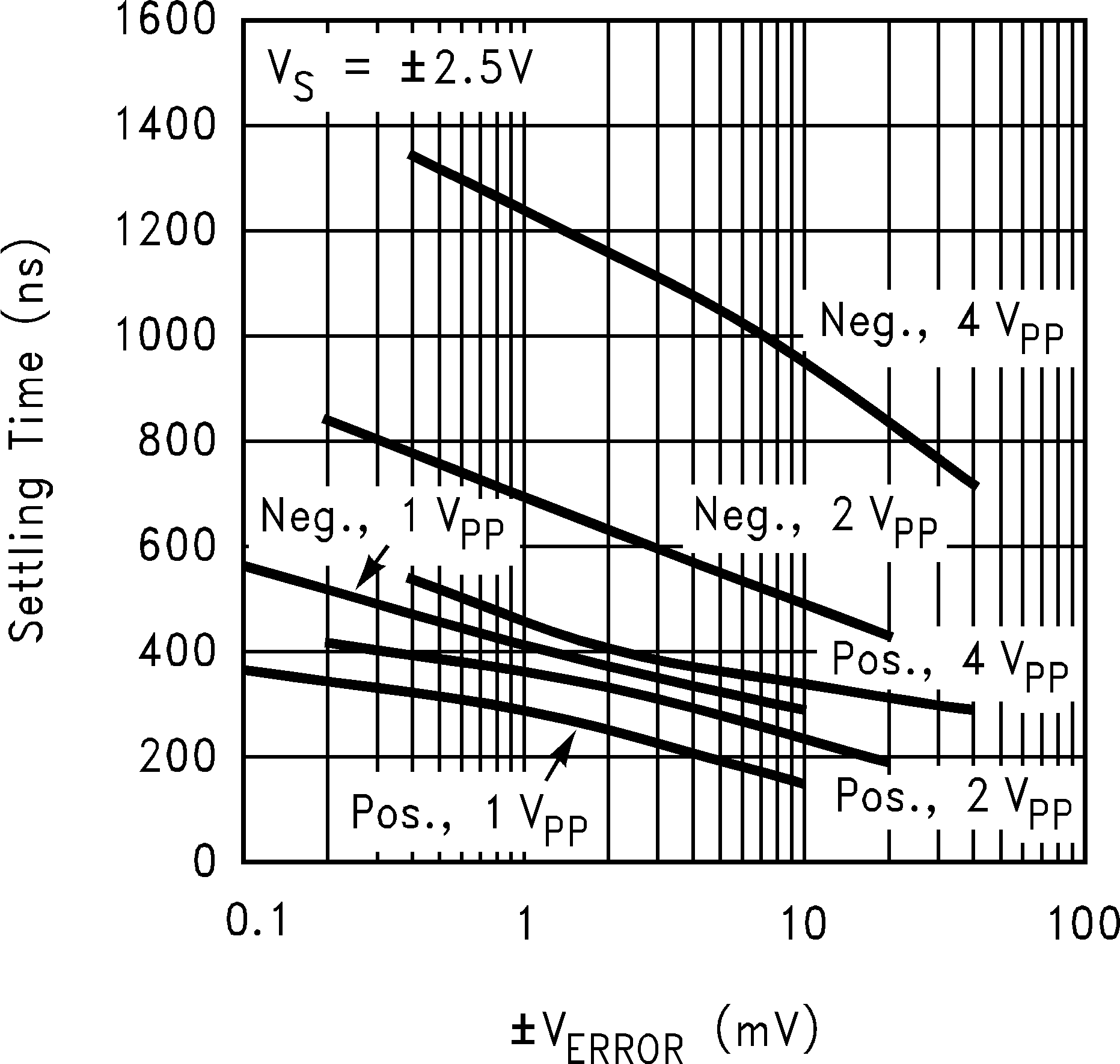
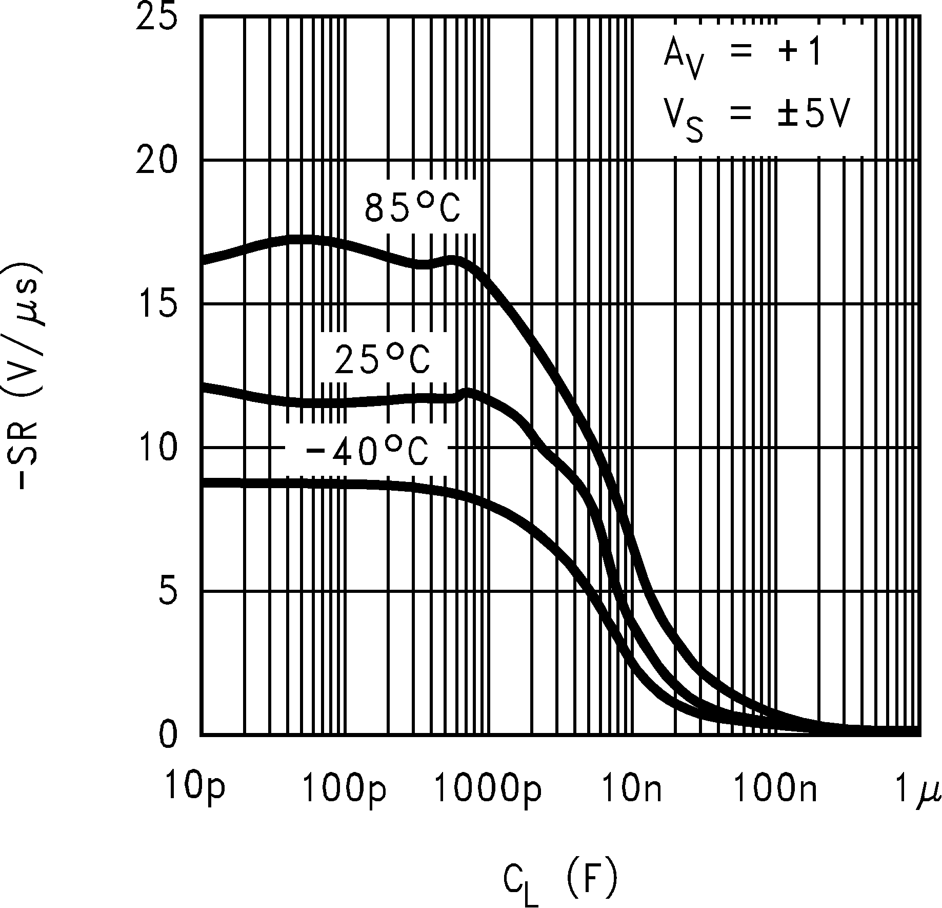
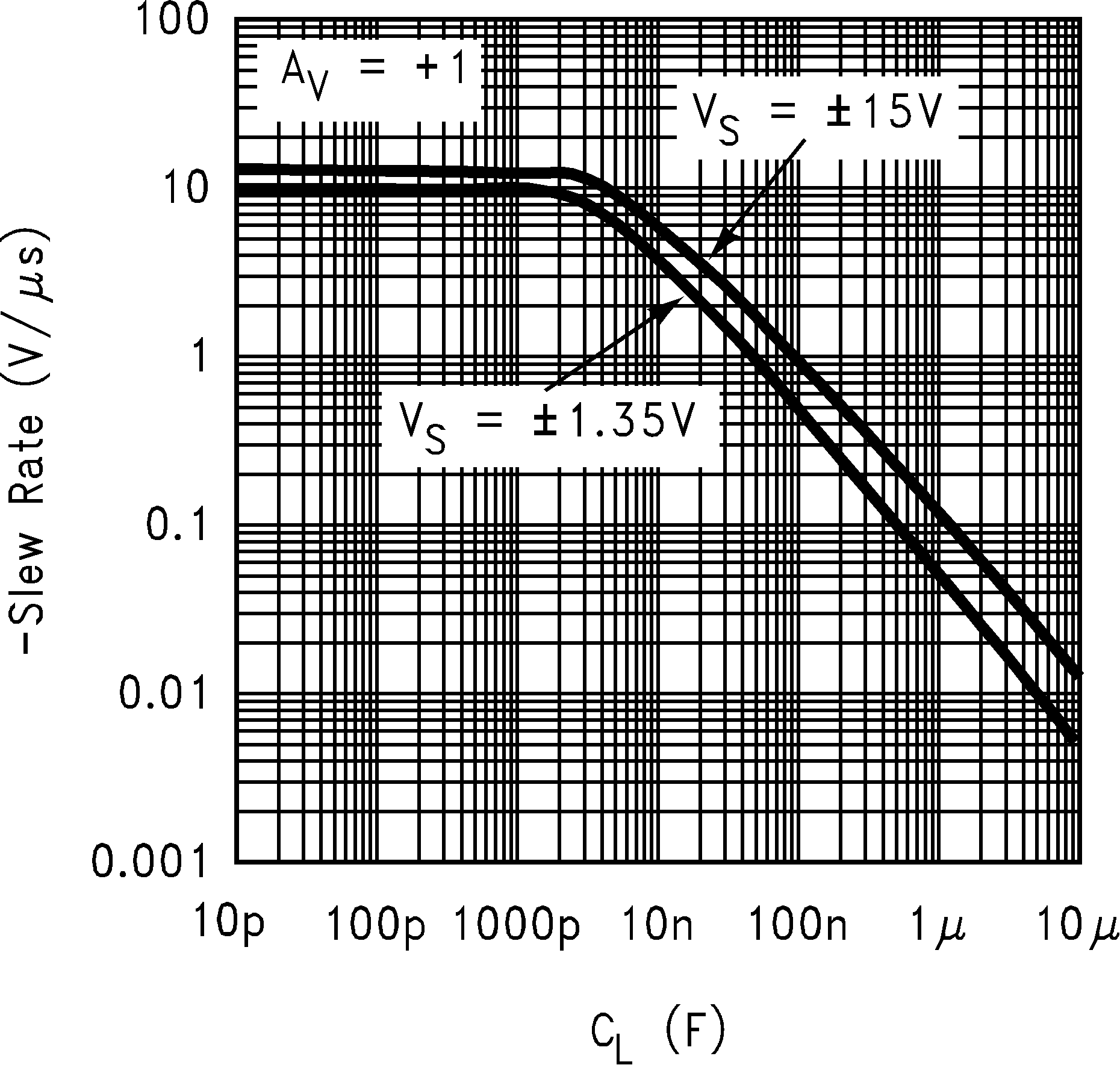
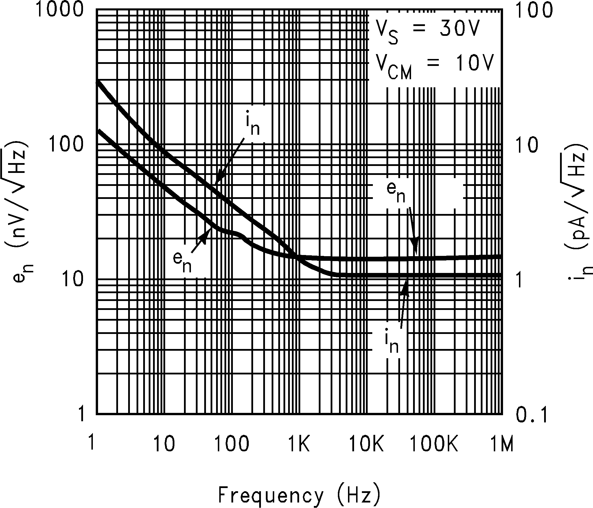
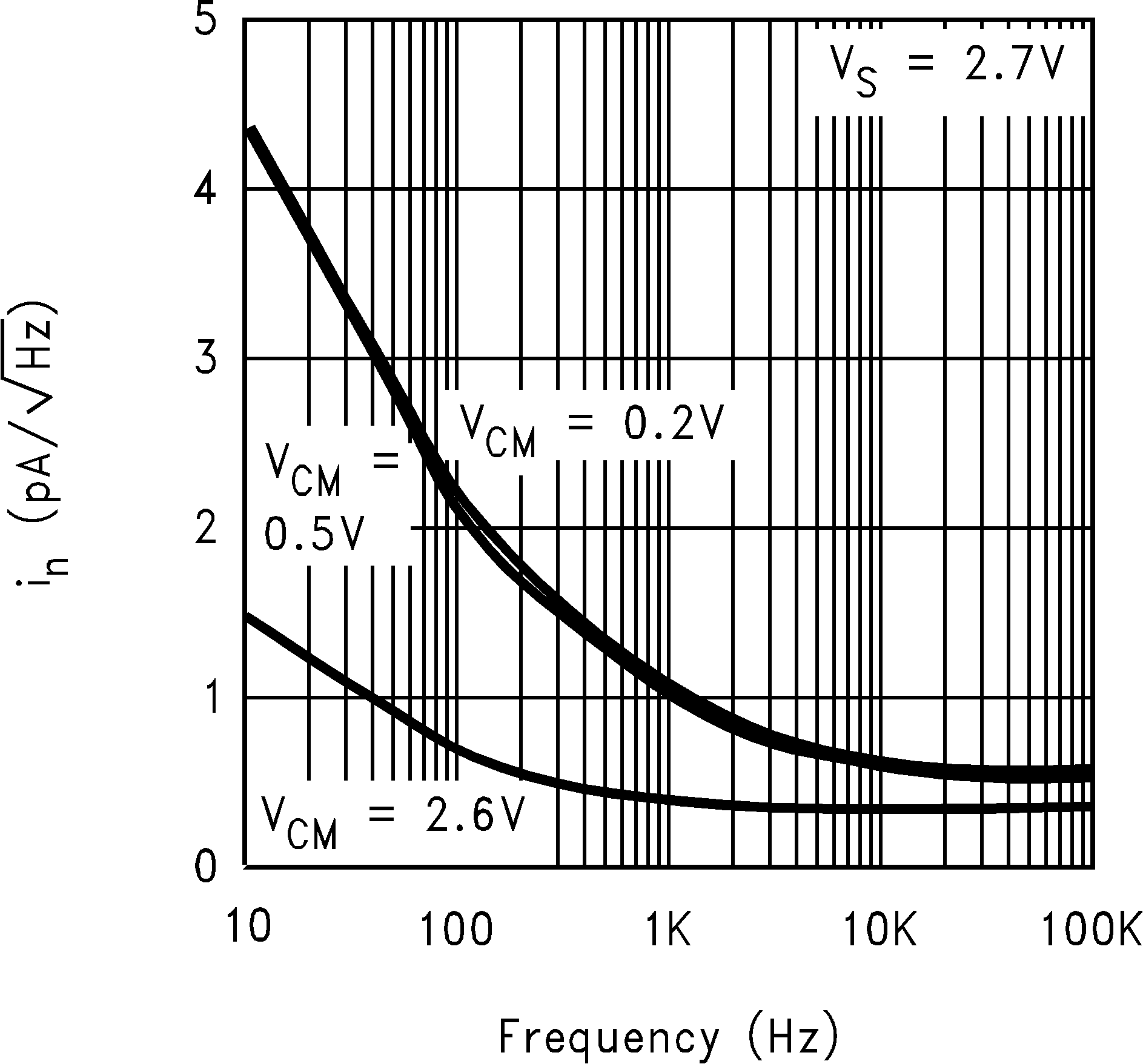
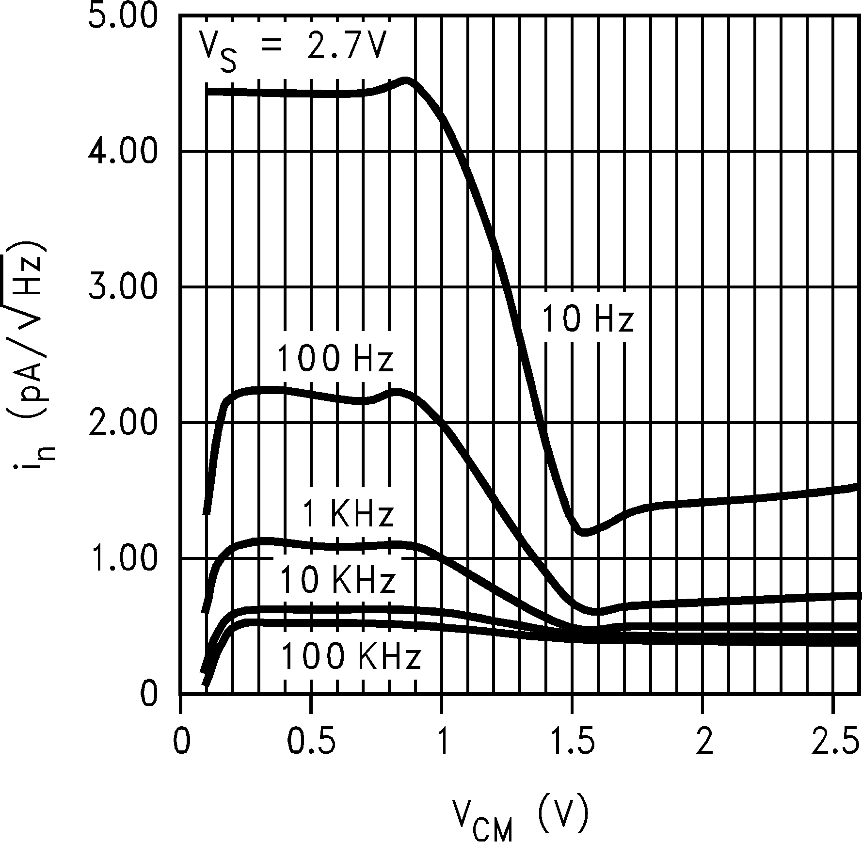
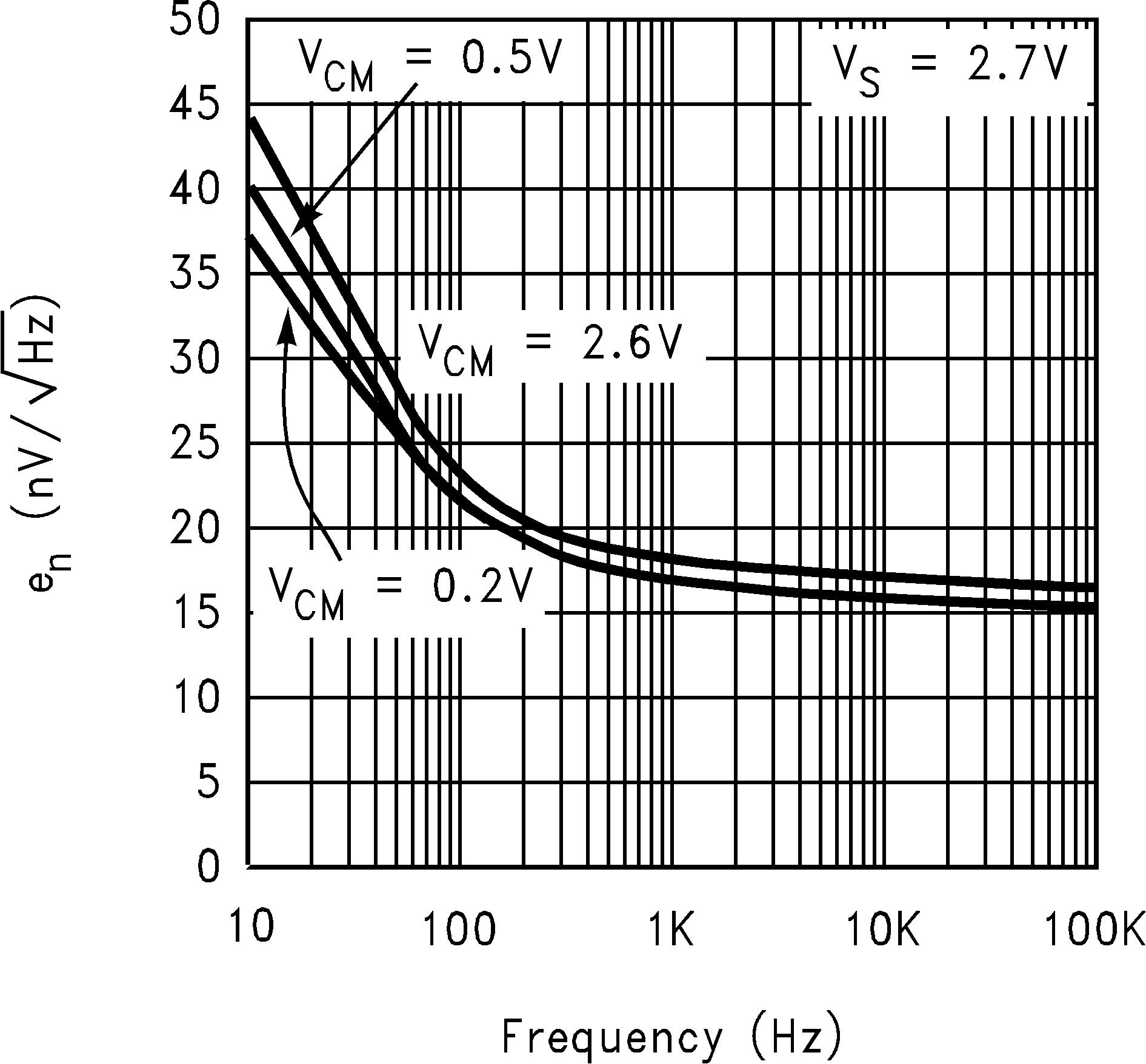
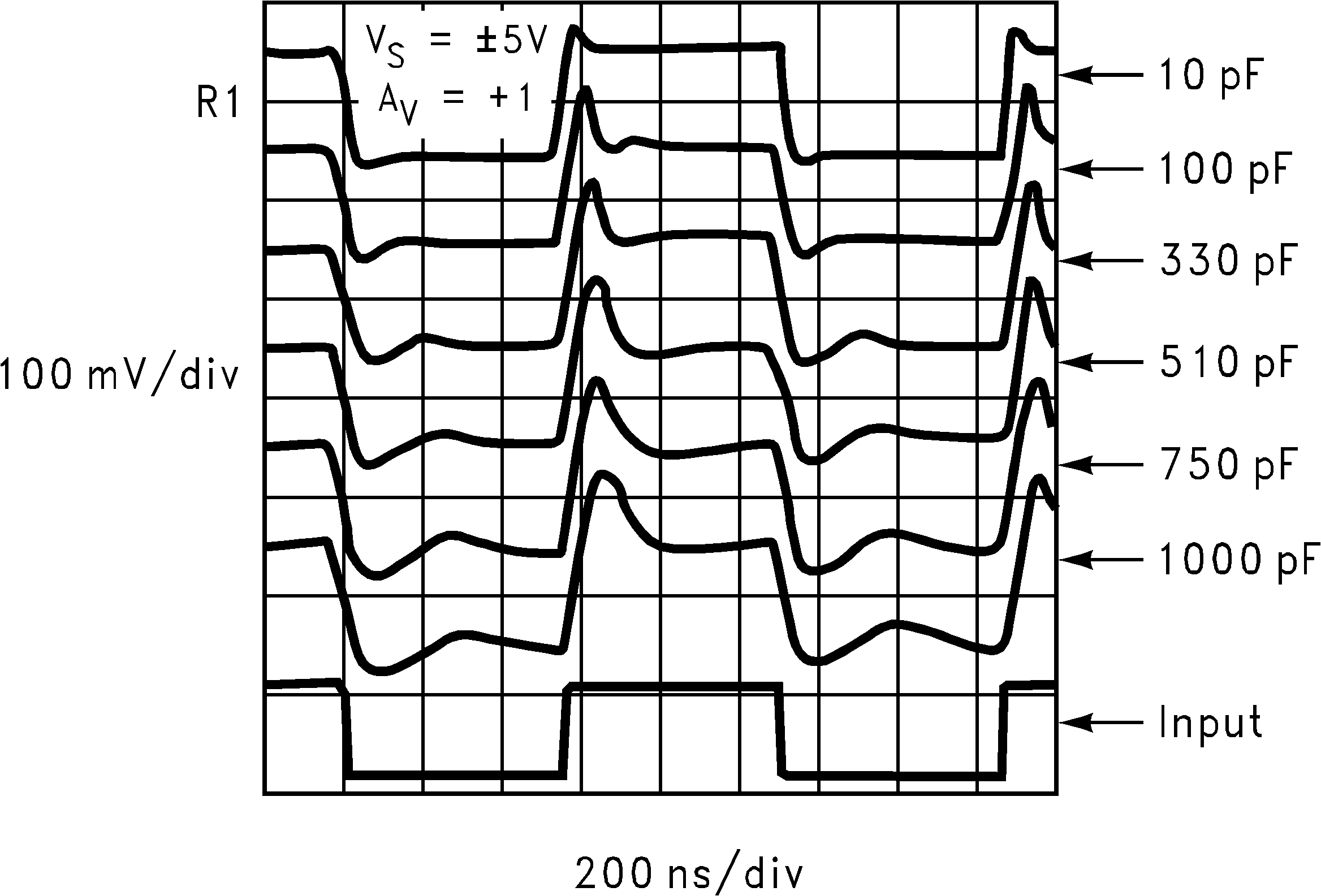
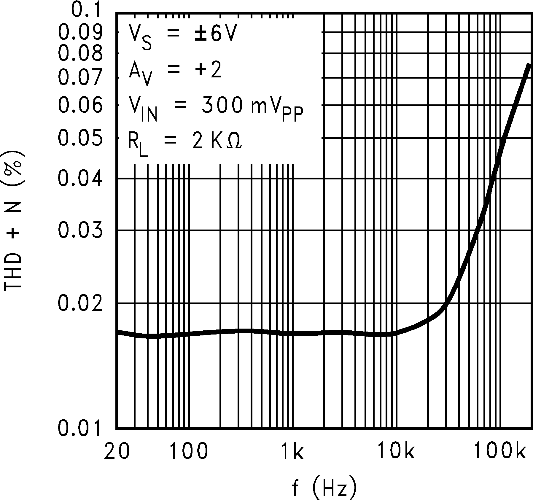
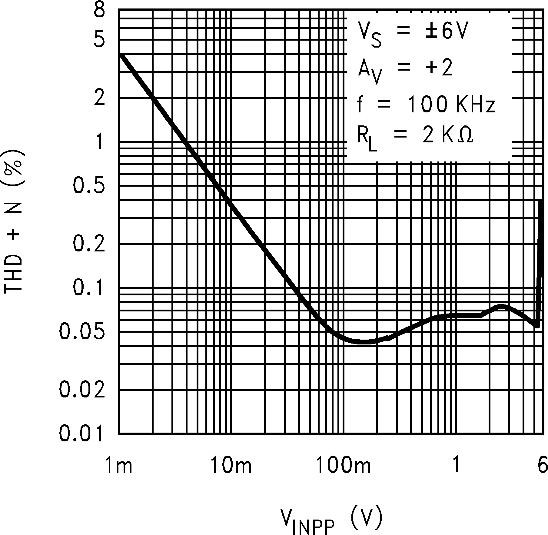
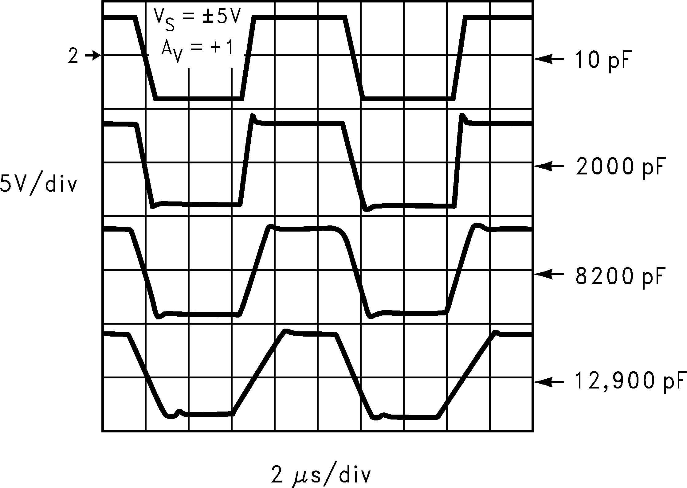
6.8 Typical Characteristics
TA = 25°C, Unless Otherwise Noted