ZHCSIK5C July 2018 – July 2019 LM5180
ADVANCE INFORMATION for pre-production products; subject to change without notice.
- 1 特性
- 2 應(yīng)用
- 3 說(shuō)明
- 4 修訂歷史記錄
- 5 Pin Configuration and Functions
- 6 Specifications
-
7 Detailed Description
- 7.1 Overview
- 7.2 Functional Block Diagram
- 7.3
Feature Description
- 7.3.1 Integrated Power MOSFET
- 7.3.2 PSR Flyback Modes of Operation
- 7.3.3 Setting the Output Voltage
- 7.3.4 Control Loop Error Amplifier
- 7.3.5 Precision Enable
- 7.3.6 Configurable Soft Start
- 7.3.7 External Bias Supply
- 7.3.8 Minimum On-Time and Off-Time
- 7.3.9 Overcurrent Protection
- 7.3.10 Thermal Shutdown
- 7.4 Device Functional Modes
-
8 Application and Implementation
- 8.1 Application Information
- 8.2
Typical Applications
- 8.2.1
Design 1: Wide VIN, Low IQ PSR Flyback Converter Rated at 5 V, 1 A
- 8.2.1.1 Design Requirements
- 8.2.1.2
Detailed Design Procedure
- 8.2.1.2.1 Custom Design With WEBENCH® Tools
- 8.2.1.2.2 Custom Design With Excel Quickstart Tool
- 8.2.1.2.3 Flyback Transformer – T1
- 8.2.1.2.4 Flyback Diode – DFLY
- 8.2.1.2.5 Zener Clamp Circuit – DF, DCLAMP
- 8.2.1.2.6 Output Capacitor – COUT
- 8.2.1.2.7 Input Capacitor – CIN
- 8.2.1.2.8 Feedback Resistor – RFB
- 8.2.1.2.9 Thermal Compensation Resistor – RTC
- 8.2.1.2.10 UVLO Resistors – RUV1, RUV2
- 8.2.1.2.11 Soft-Start Capacitor – CSS
- 8.2.1.3 Application Curves
- 8.2.2 Design 2: PSR Flyback Converter With Dual Outputs of 15 V and –7.7 V at 200 mA
- 8.2.3 Design 3: PSR Flyback Converter With Stacked Dual Outputs of 24 V and 5 V
- 8.2.1
Design 1: Wide VIN, Low IQ PSR Flyback Converter Rated at 5 V, 1 A
- 9 Power Supply Recommendations
- 10Layout
- 11器件和文檔支持
- 12"機(jī)械、封裝和可訂購(gòu)信息
封裝選項(xiàng)
機(jī)械數(shù)據(jù) (封裝 | 引腳)
- NGU|8
散熱焊盤機(jī)械數(shù)據(jù) (封裝 | 引腳)
訂購(gòu)信息
8.2.3 Design 3: PSR Flyback Converter With Stacked Dual Outputs of 24 V and 5 V
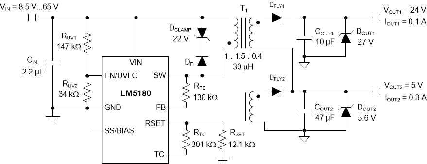
The schematic diagram of a dual-output flyback converter with high-voltage secondary stacked on the low-voltage secondary winding is given in Figure 51. This configuration reduces the number of turns for the high-voltage output, resulting in lower secondary-to-secondary leakage inductance for improved output voltage cross regulation.
 Figure 51. Schematic for Design 3 With VIN(nom) = 24 V, VOUT1 = 24 V, VOUT2 = 5 V