SNVS300H July 2004 – September 2016 LM5111
PRODUCTION DATA.
- 1 Features
- 2 Applications
- 3 Description
- 4 Revision History
- 5 Device Options
- 6 Pin Configuration and Functions
- 7 Specifications
- 8 Detailed Description
- 9 Application and Implementation
- 10Power Supply Recommendations
- 11Layout
- 12Device and Documentation Support
- 13Mechanical, Packaging, and Orderable Information
封裝選項
機械數(shù)據(jù) (封裝 | 引腳)
散熱焊盤機械數(shù)據(jù) (封裝 | 引腳)
- DGN|8
訂購信息
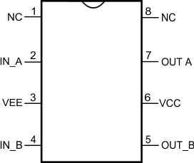
6 Pin Configuration and Functions
D and DGN Package
8-Pin SOIC and MSOP-PowerPAD
Top View

Pin Functions
| PIN | I/O | DESCRIPTION | |
|---|---|---|---|
| NAME | NO. | ||
| IN_A | 2 | I | ‘A’ side control input. TTL compatible thresholds. |
| IN_B | 4 | I | ‘B’ side control input. TTL compatible thresholds. |
| OUT_A. | 7 | O | Output for the ‘A’ side driver. Voltage swing of this output is from VCC to VEE. The output stage is capable of sourcing 3 A and sinking 5 A. |
| OUT_B | 5 | O | Output for the ‘B’ side driver. Voltage swing of this output is from VCC to VEE. The output stage is capable of sourcing 3 A and sinking 5 A. |
| VCC | 6 | — | Positive output supply. Locally decouple to VEE. |
| VEE | 3 | — | Ground reference for both inputs and outputs. Connect to power ground. |
| NC | 1, 8 | — | No Connection |
| Exposed Pad(1) | — | It is recommended that the exposed pad on the bottom of the package be soldered to ground plane on the PC board to aid thermal dissipation. | |
(1) Only available with the MSOP-PowerPAD package.