ZHCSSZ3H May 2008 – August 2023 ISO15 , ISO35
PRODUCTION DATA
- 1
- 1 特性
- 2 應(yīng)用
- 3 說明
- 4 Revision History
- 5 Pin Configuration and Functions
-
6 Specifications
- 6.1 Absolute Maximum Ratings
- 6.2 ESD Ratings
- 6.3 Recommended Operating Conditions
- 6.4 Thermal Information
- 6.5 Power Ratings
- 6.6 Insulation Specifications
- 6.7 Safety-Related Certifications
- 6.8 Safety Limiting Values
- 6.9 Electrical Characteristics: Driver
- 6.10 Electrical Characteristics: Receiver
- 6.11 Supply Current
- 6.12 Switching Characteristics: Driver
- 6.13 Switching Characteristics: Receiver
- 6.14 Insulation Characteristics Curves
- 6.15 Typical Characteristics
- 7 Parameter Measurement Information
- 8 Detailed Description
- 9 Application and Implementation
- Power Supply Recommendations
- 10Layout
- 11Device and Documentation Support
- 13Mechanical, Packaging, and Orderable Information
封裝選項(xiàng)
機(jī)械數(shù)據(jù) (封裝 | 引腳)
- DW|16
散熱焊盤機(jī)械數(shù)據(jù) (封裝 | 引腳)
訂購信息
7 Parameter Measurement Information
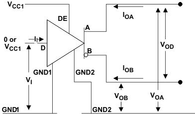 Figure 7-1 Driver VOD Test and Current Definitions
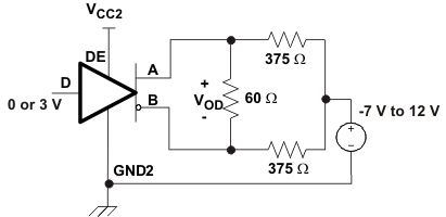 Figure 7-2 Driver VOD With Common-Mode Loading Test Circuit
 Figure 7-3 Test
Circuit and Waveform Definitions for the Driver Common-Mode Output
Voltage
 Figure 7-4 Driver
Switching Test Circuit and Voltage Waveforms
Figure 7-4 Driver
Switching Test Circuit and Voltage WaveformsNote:
Driver output pins are A and B for the ISO15 (see Figure 7-1 through Figure 7-4). These correspond to ISO35 pins Y and Z
 Figure 7-5 Driver
High-Level Output Enable and Disable Time Test Circuit and Voltage
Waveforms
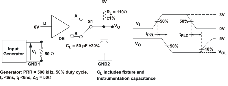 Figure 7-6 Driver
Low-Level Output Enable and Disable Time Test Circuit and Voltage
Waveform
Figure 7-6 Driver
Low-Level Output Enable and Disable Time Test Circuit and Voltage
WaveformNote:
Driver output pins are A and B for the ISO15 (see Figure 7-5 through Figure 7-6). These correspond to ISO35 pins Y and Z
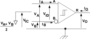 Figure 7-7 Receiver
Voltage and Current Definitions
 Figure 7-8 Receiver
Switching Test Circuit and Waveforms
 Figure 7-9 Receiver
Enable Test Circuit and Waveforms, Data Output High
 Figure 7-10 Receiver
Enable Test Circuit and Waveforms, Data Output Low
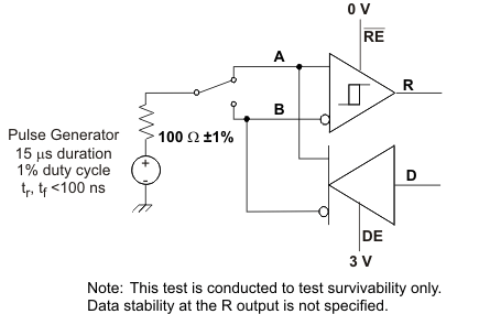 Figure 7-11 Transient
Overvoltage Test Circuit
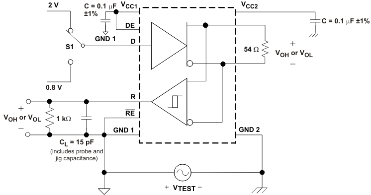 Figure 7-12 Half-Duplex Common-Mode Transient Immunity Test Circuit
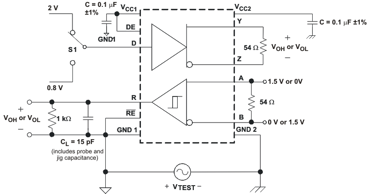 Figure 7-13 Full-Duplex Common-Mode Transient Immunity Test Circuit