SCAS859F January 2009 – June 2015 CDCLVP111
PRODUCTION DATA.
- 1 Features
- 2 Applications
- 3 Description
- 4 Revision History
- 5 Pin Configuration and Functions
- 6 Specifications
- 7 Parameter Measurement Information
- 8 Detailed Description
- 9 Applications and Implementation
- 10Power Supply Recommendations
- 11Layout
- 12Device and Documentation Support
- 13Mechanical, Packaging, and Orderable Information
封裝選項
機(jī)械數(shù)據(jù) (封裝 | 引腳)
散熱焊盤機(jī)械數(shù)據(jù) (封裝 | 引腳)
- RHB|32
訂購信息
7 Parameter Measurement Information
7.1 Test Configurations

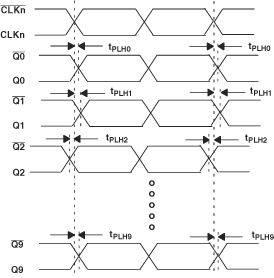
A. Output skew is calculated as the greater of: The difference between the fastest and the slowest tPLHn (n = 0, 1,...9) or the difference between the fastest and the slowest tPHLn (n = 0, 1,...9).
B. Part-to-part skew, is calculated as the greater of: The difference between the fastest and the slowest tPLHn (n = 0, 1,...9) across multiple devices or the difference between the fastest and the slowest tPHLn (n = 0, 1,...9) across multiple devices.
C. Typical value measured at ambient when clock input is 155.52 MHz for an integration bandwidth of 20 kHz to 5 MHz.
D. Input conditions: VCM = 1 V, VID = 0.5 V and FIN = 1 GHz.
Figure 2. Waveform for Calculating Both Output and Part-to-Part Skew
 Figure 3. Output Voltage and Rise and Fall Time
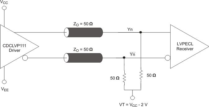
 Figure 4. Typical Termination for Output Driver (See the Interfacing Between LVPECL, LVDS, and CML Application Note, SCAA056)
 Figure 5. LVPECL Output DC Configuration During Device Test
 Figure 6. LVPECL Output AC Configuration During Device Test