SCAS884D August 2009 – December 2015 CDCLVP1102
PRODUCTION DATA.
- 1 Features
- 2 Applications
- 3 Description
- 4 Revision History
- 5 Pin Configuration and Functions
-
6 Specifications
- 6.1 Absolute Maximum Ratings
- 6.2 ESD Ratings
- 6.3 Recommended Operating Conditions
- 6.4 Thermal Information
- 6.5 Electrical Characteristics: LVCMOS Input
- 6.6 Electrical Characteristics: Differential Input
- 6.7 Electrical Characteristics: LVPECL Output
- 6.8 Electrical Characteristics: LVPECL Output
- 6.9 Typical Characteristics
- 7 Parameter Measurement Information
- 8 Detailed Description
- 9 Application and Implementation
- 10Power Supply Recommendations
- 11Layout
- 12Device and Documentation Support
- 13Mechanical, Packaging, and Orderable Information
封裝選項
機械數(shù)據(jù) (封裝 | 引腳)
- RGT|16
散熱焊盤機械數(shù)據(jù) (封裝 | 引腳)
- RGT|16
訂購信息
7 Parameter Measurement Information
7.1 Test Configurations
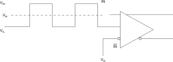
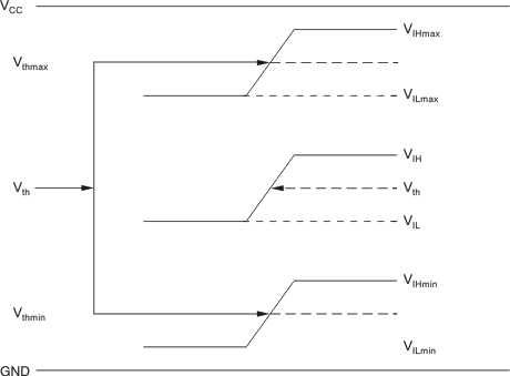
This section describes the function of each block for the CDCLVP1102. Figure 3 through Figure 9 illustrate how the device should be setup for a variety of test configurations.
 Figure 3. DC-Coupled LVCMOS Input During Device Test
 Figure 4. Vth Variation Over LVCMOS Levels
 Figure 5. DC-Coupled LVPECL Input During Device Test
 Figure 6. DC-Coupled LVDS Input During Device Test
 Figure 7. AC-Coupled Differential Input to Device
 Figure 8. LVPECL Output DC Configuration During Device Test
 Figure 9. LVPECL Output AC Configuration During Device Test
Figure 10 shows the output voltage and rise/fall time. Output and part-to-part skew are shown in Figure 11.
 Figure 10. Output Voltage and Rise/Fall Time

1. Output skew is calculated as the greater of the following: As the difference between the fastest and the slowest tPLHn (n = 0, 1), or as the difference between the fastest and the slowest tPHLn (n = 0, 1).
2. Part-to-part skew is calculated as the greater of the following: As the difference between the fastest and the slowest tPLHn (n = 0, 1) across multiple devices, or the difference between the fastest and the slowest tPHLn (n = 0, 1) across multiple devices.
Figure 11. Output and Part-to-Part Skew