SCAS899A August 2010 – October 2016 CDCLVD1208
PRODUCTION DATA.
- 1 Features
- 2 Applications
- 3 Description
- 4 Revision History
- 5 Pin Configuration and Functions
- 6 Specifications
- 7 Parameter Measurement Information
- 8 Detailed Description
- 9 Application and Implementation
- 10Power Supply Recommendations
- 11Layout
- 12Device and Documentation Support
- 13Mechanical, Packaging, and Orderable Information
封裝選項(xiàng)
機(jī)械數(shù)據(jù) (封裝 | 引腳)
- RHD|28
散熱焊盤機(jī)械數(shù)據(jù) (封裝 | 引腳)
- RHD|28
訂購信息
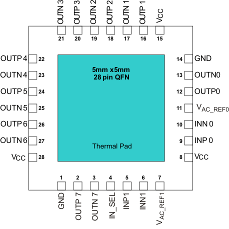
5 Pin Configuration and Functions
RHD Package
28-Pin VQFN
Top View

Pin Functions
| PIN | TYPE(1) | DESCRIPTION | |
|---|---|---|---|
| NO. | NAME | ||
| 1, 14 | GND | G | Device ground |
| 2, 3 | OUTP7, OUTN7 | O | Differential LVDS output pair number 7 |
| 4 | IN_SEL | I | Input Selection with an internal 200-kΩ pullup and pulldown, selects input port; (See Table 1) |
| 5, 6 | INP1, INN1 | I | Differential redundant input pair or single-ended input |
| 7 | VAC_REF1 | O | Bias voltage output for capacitive coupled inputs. If used, TI recommends using a 0.1-µF capacitor to GND on this pin. |
| 8, 15, 28 | VCC | P | 2.5-V supplies for the device |
| 9, 10 | INP0, INN0 | I | Differential input pair or single-ended input |
| 11 | VAC_REF0 | O | Bias voltage output for capacitive coupled inputs. If used, TI recommends using a 0.1-µF capacitor to GND on this pin. |
| 12, 13 | OUTP0, OUTN0 | O | Differential LVDS output pair number 0 |
| 16, 17 | OUTP1, OUTN1 | O | Differential LVDS output pair number 1 |
| 18, 19 | OUTP2, OUTN2 | O | Differential LVDS output pair number 2 |
| 20, 21 | OUTP3, OUTN3 | O | Differential LVDS output pair number 3 |
| 22, 23 | OUTP4, OUTN4 | O | Differential LVDS output pair number 4 |
| 24, 25 | OUTP5, OUTN5 | O | Differential LVDS output pair number 5 |
| 26, 27 | OUTP6, OUTN6 | O | Differential LVDS output pair number 6 |
(1) G = Ground, I = Input, O = Output, P = Power