SCAS841D February 2007 – December 2016 CDCLVD110A
PRODUCTION DATA.
- 1 Features
- 2 Applications
- 3 Description
- 4 Revision History
- 5 Pin Configuration and Functions
- 6 Specifications
- 7 Parameter Measurement Information
- 8 Detailed Description
- 9 Application and Implementation
- 10Power Supply Recommendations
- 11Layout
- 12Device and Documentation Support
- 13Mechanical, Packaging, and Orderable Information
封裝選項(xiàng)
機(jī)械數(shù)據(jù) (封裝 | 引腳)
散熱焊盤(pán)機(jī)械數(shù)據(jù) (封裝 | 引腳)
- RHB|32
訂購(gòu)信息
7 Parameter Measurement Information

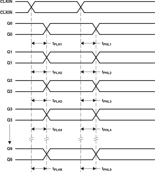
A. Output skew, tsk(o), is calculated as the greater of:
– The difference between the fastest and the slowest tPLHn (n = 1, 2,...10)
– The difference between the fastest and the slowest tPHLn (n = 1, 2,...10)
– The difference between the fastest and the slowest tPLHn (n = 1, 2,...10)
– The difference between the fastest and the slowest tPHLn (n = 1, 2,...10)
B. Part-to-part skew, tsk(pp), is calculated as the greater of:
– The difference between the fastest and the slowest tPLHn (n = 1, 2,...10) across multiple devices
– The difference between the fastest and the slowest tPHLn (n = 1, 2,...10) across multiple devices
– The difference between the fastest and the slowest tPLHn (n = 1, 2,...10) across multiple devices
– The difference between the fastest and the slowest tPHLn (n = 1, 2,...10) across multiple devices
C. Pulse skew, tsk(p), is calculated as the magnitude of the absolute time difference between the high-to-low (tPHL) and the low-to-high (tPLH) propagation delays when a single switching input causes one or more outputs to switch,
tsk(p) = | tPHL – tPLH |. Pulse skew is sometimes referred to as pulse-width distortion or duty-cycle skew.
Figure 2. Waveforms for Calculation of tsk(o) and tsk(pp)
tsk(p) = | tPHL – tPLH |. Pulse skew is sometimes referred to as pulse-width distortion or duty-cycle skew.
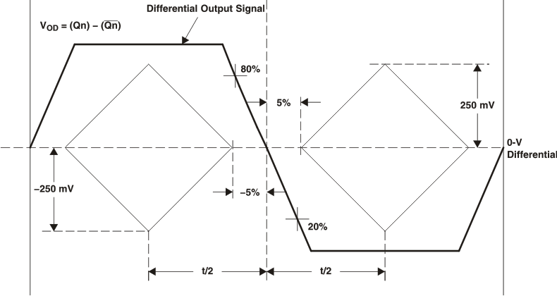
 Figure 3. Test Criteria for fclk, Duty Cycle, tr, tf, VOD
 Figure 4. LVDS Output DC Configuration During Device Test
 Figure 5. LVDS Output AC Configuration During Device Test
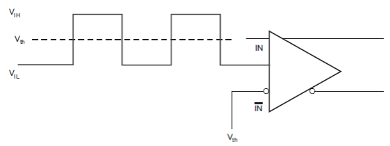
 Figure 6. DC-Coupled LVCMOS Input During Device Test
 Figure 7. Output Voltage and Rise/Fall Time