SLUSA78C July 2010 – July 2015
PRODUCTION DATA.
- 1 Features
- 2 Applications
- 3 Description
- 4 Revision History
- 5 Device Comparison Table
- 6 Pin Configuration and Functions
- 7 Specifications
-
8 Detailed Description
- 8.1 Overview
- 8.2 Functional Block Diagram
- 8.3
Feature Description
- 8.3.1 Automatic Internal Soft-Start Charger Current
- 8.3.2 High-Accuracy Current-Sense Amplifier
- 8.3.3 Charge Timeout
- 8.3.4 Input Overcurrent Protection (ACOC)
- 8.3.5 Charge Overcurrent Protection (CHGOCP)
- 8.3.6 Battery Overvoltage Protection (BATOVP)
- 8.3.7 Battery Shorted to Ground (BATLOWV)
- 8.3.8 Thermal Shutdown Protection (TSHUT)
- 8.4 Device Functional Modes
- 8.5
Programming
- 8.5.1 SMBus Interface
- 8.5.2 Battery-Charger Commands
- 8.5.3 Setting Charger Options
- 8.5.4 Setting the Charge Current
- 8.5.5 Setting the Charge Voltage
- 8.5.6 Setting Input Current
- 8.5.7 Adapter Detect and ACOK Output
- 8.5.8 Converter Operation
- 8.5.9 EMI Switching Frequency Adjust
- 8.5.10 Inductor Short, MOSFET Short Protection
- 8.5.11 Independent Comparator
- 9 Application and Implementation
- 10Power Supply Recommendations
- 11Layout
- 12Device and Documentation Support
- 13Mechanical, Packaging, and Orderable Information
7 Specifications
7.1 Absolute Maximum Ratings
over operating free-air temperature range (unless otherwise noted)(1)(2)| MIN | MAX | UNIT | ||
|---|---|---|---|---|
| Voltage | SRN, SRP, ACN, ACP, VCC | –0.3 | 30 | V |
| PHASE | –2 | 30 | ||
| ACDET, SDA, SCL, LODRV, REGN, IOUT, ILIM, ACOK, IFAULT, CMPIN, CMPOUT | –0.3 | 7 | ||
| BTST, HIDRV | –0.3 | 36 | ||
| Maximum difference voltage | SRP–SRN, ACP–ACN | –0.5 | 0.5 | |
| Junction temperature, TJ | –40 | 155 | °C | |
| Storage temperature, Tstg | –55 | 155 | °C | |
(1) Stresses beyond those listed under Absolute Maximum Ratings may cause permanent damage to the device. These are stress ratings only, which do not imply functional operation of the device at these or any other conditions beyond those indicated under Recommended Operating Conditions. Exposure to absolute-maximum-rated conditions for extended periods may affect device reliability.
(2) All voltages are with respect to GND if not specified. Currents are positive into, negative out of the specified terminal. Consult Packaging Section of the data book for thermal limitations and considerations of packages.
7.2 ESD Ratings
| VALUE | UNIT | |||
|---|---|---|---|---|
| V(ESD) | Electrostatic discharge | Human body model (HBM), per ANSI/ESDA/JEDEC JS-001(1) | ±2000 | V |
| Charged device model (CDM), per JEDEC specification JESD22-C101(2) | ±500 | |||
(1) JEDEC document JEP155 states that 500-V HBM allows safe manufacturing with a standard ESD control process.
(2) JEDEC document JEP157 states that 250-V CDM allows safe manufacturing with a standard ESD control process.
7.3 Recommended Operating Conditions
over operating free-air temperature range (unless otherwise noted)| MIN | NOM | MAX | UNIT | ||
|---|---|---|---|---|---|
| Voltage | SRN, SRP, ACN, ACP, VCC | 0 | 24 | V | |
| PHASE | –2 | 24 | |||
| ACDET, SDA, SCL, LODRV, REGN, IOUT, ILIM, ACOK, IFAULT, CMPIN, CMPOUT | 0 | 6.5 | |||
| BTST, HIDRV | 0 | 30 | |||
| Maximum difference voltage | SRP–SRN, ACP–ACN | –0.2 | 0.2 | V | |
| Junction temperature, TJ | 0 | 125 | °C | ||
7.4 Thermal Information
| THERMAL METRIC(1) | bq24707x | UNIT | |
|---|---|---|---|
| RGR [VQFN] | |||
| 20 PINS | |||
| RθJA | Junction-to-ambient thermal resistance | 46.8 | °C/W |
| RθJC(top) | Junction-to-case (top) thermal resistance | 56.9 | °C/W |
| RθJB | Junction-to-board thermal resistance | 46.6 | °C/W |
| ψJT | Junction-to-top characterization parameter | 0.6 | °C/W |
| ψJB | Junction-to-board characterization parameter | 15.3 | °C/W |
| RθJC(bot) | Junction-to-case (bottom) thermal resistance | 4.4 | °C/W |
(1) For more information about traditional and new thermal metrics, see the Semiconductor and IC Package Thermal Metrics application report, SPRA953.
7.5 Electrical Characteristics
4.5 V ≤ V(VCC) ≤ 24 V, 0°C ≤ TJ ≤ 125°C, typical values are at TA = 25°C, with respect to GND (unless otherwise noted)| PARAMETER | TEST CONDITIONS | MIN | TYP | MAX | UNIT | |
|---|---|---|---|---|---|---|
| OPERATING CONDITIONS | ||||||
| VVCC_OP | VCC Input voltage operating | 4.5 | 24 | V | ||
| CHARGE VOLTAGE REGULATION | ||||||
| VBAT_REG_RNG | BAT voltage regulation | 1.024 | 19.2 | V | ||
| VBAT_REG_ACC | Charge voltage regulation accuracy | ChargeVoltage() = 0x41A0H | 16.716 | 16.8 | 16.884 | V |
| –0.5% | 0.5% | |||||
| ChargeVoltage() = 0x3130H | 12.529 | 12.592 | 12.655 | V | ||
| –0.5% | 0.5% | |||||
| ChargeVoltage() = 0x20D0H | 8.35 | 8.4 | 8.45 | V | ||
| –0.6% | 0.6% | |||||
| ChargeVoltage() = 0x1060H | 4.163 | 4.192 | 4.221 | V | ||
| –0.7% | 0.7% | |||||
| CHARGE CURRENT REGULATION | ||||||
| VIREG_CHG_RNG | Charge current regulation differential voltage | VIREG_CHG = VSRP - VSRN | 0 | 81.28 | mV | |
| ICHRG_REG_ACC | Charge current regulation accuracy 10-mΩ current-sensing resistor | ChargeCurrent() = 0x1000H | 3973 | 4096 | 4219 | mA |
| –3% | 3% | |||||
| ChargeCurrent() = 0x0800H | 1946 | 2048 | 2150 | mA | ||
| –5% | 5% | |||||
| ChargeCurrent() = 0x0200H | 410 | 512 | 614 | mA | ||
| –20% | 20% | |||||
| ChargeCurrent() = 0x0100H | 172 | 256 | 340 | mA | ||
| –33% | 33% | |||||
| ChargeCurrent() = 0x0080H | 64 | 128 | 192 | mA | ||
| –50% | 50% | |||||
| INPUT CURRENT REGULATION | ||||||
| VIREG_DPM_RNG | Input current regulation differential voltage | VIREG_DPM = VACP – VACN | 0 | 80.64 | mV | |
| IDPM_REG_ACC | Input current regulation accuracy 10-mΩ current-sensing resistor |
InputCurrent() = 0x1000H | 3973 | 4096 | 4219 | mA |
| –3% | 3% | |||||
| InputCurrent() = 0x0800H | 1946 | 2048 | 2150 | mA | ||
| –5% | 5% | |||||
| InputCurrent() = 0x0400H | 870 | 1024 | 1178 | mA | ||
| –15% | 15% | |||||
| InputCurrent() = 0x0200H | 384 | 512 | 640 | mA | ||
| –25% | 25% | |||||
| INPUT CURRENT OR CHARGE CURRENT-SENSE AMPLIFIER | ||||||
| VACP/N_OP | Input common mode | Voltage on ACP/ACN | 4.5 | 24 | V | |
| VSRP/N_OP | Output common mode | Voltage on SRP/SRN | 0 | 19.2 | V | |
| VIOUT | IOUT output voltage | 0 | 1.6 | V | ||
| IIOUT | IOUT output current | 0 | 1 | mA | ||
| AIOUT | Current-sense amplifier gain | V(ICOUT)/V(SRP-SRN) or V(ACP-ACN) | 20 | V/V | ||
| VIOUT_ACC | Current-sense output accuracy | V(SRP-SRN) or V(ACP-ACN) = 40.96 mV | –2% | 2% | ||
| V(SRP-SRN) or V(ACP-ACN) = 20.48 mV | –4% | 4% | ||||
| V(SRP-SRN) or V(ACP-ACN) = 10.24 mV | –15% | 15% | ||||
| V(SRP-SRN) or V(ACP-ACN) = 5.12 mV | –20% | 20% | ||||
| V(SRP-SRN) or V(ACP-ACN) = 2.56 mV | –33% | 33% | ||||
| V(SRP-SRN) or V(ACP-ACN) = 1.28 mV | –50% | 50% | ||||
| CIOUT_MAX | Maximum output load capacitance | For stability with 0- to 1-mA load | 100 | pF | ||
| REGN REGULATOR | ||||||
| VREGN_REG | REGN regulator voltage | VVCC > 6.5 V, VACDET > 0. 6V (0-55 mA load) | 5.5 | 6 | 6.5 | V |
| IREGN_LIM | REGN current limit | VREGN = 0 V, VVCC > UVLO charge enabled and not in TSHUT | 65 | 80 | mA | |
| IREGN_LIM_TSHUT | VREGN = 0 V, VVCC > UVLO charge disabled or in TSHUT | 7 | 16 | |||
| CREGN | REGN output capacitor required for stability | ILOAD = 100 µA to 65 mA | 1 | µF | ||
| INPUT UNDERVOLTAGE LOCKOUT COMPARATOR (UVLO) | ||||||
| VUVLO | Input undervoltage rising threshold | VVCC rising | 3.5 | 3.75 | 4 | V |
| VUVLO_HYS | Input undervoltage falling hysteresis | VVCC falling | 340 | mV | ||
| FAST DPM COMPARATOR (FAST_DPM) | ||||||
| VFAST_DPM | Fast DPM comparator stop charging rising threshold with respect to input current limit, voltage across input sense resistor rising edge (specified by design) | 108% | ||||
| QUIESCENT CURRENT | ||||||
| IBAT | Total battery leakage current to ISRN + ISRP +IPHASE + IVCC + IACP + IACN | VVCC < VBAT = 16.8 V, TJ = 0 to 85°C | 15 | µA | ||
| ISTANDBY | Standby quiescent current, IVCC + IACP + IACN | VVCC > VUVLO, VACDET > 0.6 V, charge disabled, TJ = 0 to 85°C |
0.5 | 1 | mA | |
| IAC_NOSW | Adapter bias current during charge, IVCC + IACP + IACN |
VVCC > VUVLO, VACDET > 2.4 V, charge enabled, no switching, TJ = 0 to 85°C |
1.5 | 3 | mA | |
| IAC_SW | Adapter bias current during charge, IVCC + IACP + IACN |
VVCC > VUVLO, VACDET > 2.4 V, charge enabled, switching, MOSFET Sis412DN |
10 | mA | ||
| ACOK COMPARATOR | ||||||
| VACOK_FALL | ACOK falling threshold | VVCC>VUVLO, VACDET rising | 2.376 | 2.4 | 2.424 | V |
| VACOK_RISE_HYS | ACOK rising hysteresis | VVCC>VUVLO, VACDET falling | 35 | 55 | 75 | mV |
| VWAKEUP_RISE | WAKEUP detect rising threshold | VVCC>VUVLO, VACDET rising | 0.57 | 0.8 | V | |
| VWAKEUP_FALL | WAKEUP detect falling threshold | VVCC>VUVLO, VACDET falling | 0.3 | 0.51 | V | |
| VCC to SRN COMPARATOR (VCC_SRN) | ||||||
| VVCC-SRN_FALL | VCC-SRN falling threshold | VVCC falling towards VSRN | 70 | 125 | 180 | mV |
| VVCC-SRN _RHYS | VCC-SRN rising hysteresis | VVCC rising above VSRN | 70 | 120 | 170 | mV |
| HIGH-SIDE IFAULT COMPARATOR (IFAULT_HI)(1) | ||||||
| VIFAULT_HI_RISE | ACP to PHASE rising threshold | ChargeOption() bit [8:7] = 00 | 200 | 300 | 450 | mV |
| ChargeOption() bit [8:7] = 01 | 330 | 500 | 700 | |||
| ChargeOption() bit [8:7] = 10 (default) | 450 | 700 | 1000 | |||
| ChargeOption() bit [8:7] = 11 | 600 | 900 | 1250 | |||
| LOW-SIDE IFAULT COMPARATOR (IFAULT_LOW) | ||||||
| VIFAULT_LOW_RISE | PHASE to GND rising threshold | 40 | 110 | 160 | mV | |
| INPUT OVERCURRENT COMPARATOR (ACOC)(1) | ||||||
| VACOC | Adapter overcurrent rising threshold with respect to input current limit, voltage across input sense resistor rising edge | ChargeOption() bit [2:1] = 01 | 120% | 133% | 145% | |
| ChargeOption() bit [2:1] = 10 (default) | 150% | 166% | 180% | |||
| ChargeOption() bit [2:1] = 11 | 200% | 222% | 240% | |||
| VACOC_min | Min ACOC threshold clamp voltage | ChargeOption() bit [2:1] = 01 (133%), InputCurrent() = 0x0400H (10.24mV) |
40 | 45 | 50 | mV |
| VACOC_max | Max ACOC threshold clamp voltage | ChargeOption() bit [2:1] = 11 (222%), InputCurrent() = 0x1F80H (80.64mV) |
140 | 150 | 160 | mV |
| tACOC_DEG | ACOC deglitch time (specified by design) | Voltage across input sense resistor rising to disable charge | 1.7 | 2.5 | 3.3 | ms |
| BAT OVERVOLTAGE COMPARATOR (BAT_OVP) | ||||||
| VOVP_RISE | Overvoltage rising threshold as percentage of VBAT_REG | VSRN rising | 103% | 104% | 106% | |
| VOVP_FALL | Overvoltage falling threshold as percentage of VBAT_REG | VSRN falling | 102% | |||
| CHARGE OVERCURRENT COMPARATOR (CHG_OCP) | ||||||
| VOCP_RISE | Charge overcurrent rising threshold, measure voltage drop across current-sensing resistor | ChargeCurrent() = 0x0xxxH | 54 | 60 | 66 | mV |
| ChargeCurrent() = 0x1000H – 0x17C0H | 80 | 90 | 100 | mV | ||
| ChargeCurrent() = 0x1800 H– 0x1FC0H | 110 | 120 | 130 | mV | ||
| CHARGE UNDERCURRENT COMPARATOR (CHG_UCP) | ||||||
| VUCP_FALL | Charge undercurrent falling threshold | VSRP falling towards VSRN | 1 | 5 | 9 | mV |
| LIGHT LOAD COMPARATOR (LIGHT_LOAD) | ||||||
| VLL_FALL | Light load falling threshold | Measure voltage drop across current-sensing resistor | 1.25 | mV | ||
| VLL_RISE_HYST | Light load rising hysteresis | Measure voltage drop across current-sensing resistor | 1.25 | mV | ||
| BATTERY LOWV COMPARATOR (BAT_LOWV) | ||||||
| VBATLV_FALL | Battery LOWV falling threshold | VSRN falling | 2.4 | 2.5 | 2.6 | V |
| VBATLV_RHYST | Battery LOWV rising hysteresis | VSRN rising | 200 | mV | ||
| IBATLV | Battery LOWV charge current limit | 10-mΩ current sensing resistor | 0.5 | A | ||
| THERMAL SHUTDOWN COMPARATOR (TSHUT) | ||||||
| TSHUT | Thermal shutdown rising temperature | Temperature rising | 155 | °C | ||
| TSHUT_HYS | Thermal shutdown hysteresis, falling | Temperature falling | 20 | °C | ||
| ILIM COMPARATOR | ||||||
| VILIM_FALL | ILIM as CE falling threshold | VILIM falling | 60 | 75 | 90 | mV |
| VILIM_RISE | ILIM as CE rising threshold | VILIM rising | 90 | 105 | 120 | mV |
| LOGIC INPUT (SDA, SCL) | ||||||
| VIN_ LO | Input low threshold | 0.8 | V | |||
| VIN_ HI | Input high threshold | 2.1 | V | |||
| IIN_ LEAK | Input bias current | V = 7 V | –1 | 1 | μA | |
| LOGIC OUTPUT OPEN DRAIN (ACOK, SDA, IFAULT, CMPOUT) | ||||||
| VOUT_ LO | Output saturation voltage | 5-mA drain current | 500 | mV | ||
| IOUT_ LEAK | Leakage current | V = 7 V | –1 | 1 | μA | |
| ANALOG INPUT (ACDET, ILIM) | ||||||
| IIN_ LEAK | Input bias current | V = 7 V | –1 | 1 | μA | |
| ANALOG INPUT (CMPIN has 50-kΩ series resistor and 2000-kΩ pulldown resistor) | ||||||
| IIN_LEAK | Input bias current | V = 7 V | 1 | 3.5 | 7 | μA |
| PWM OSCILLATOR | ||||||
| FSW | PWM switching frequency | ChargeOption() bit [9] = 0 (default) | 600 | 750 | 900 | kHz |
| FSW+ | PWM increase frequency | ChargeOption() bit [10:9] = 11 | 665 | 885 | 1100 | kHz |
| FSW– | PWM decrease frequency | ChargeOption() bit [10:9] = 01 | 465 | 615 | 765 | kHz |
| PWM HIGH-SIDE DRIVER (HIDRV) | ||||||
| RDS_HI_ON | High-side driver (HSD) turnon resistance | VBTST – VPH = 5.5 V, I = 10mA | 12 | 20 | Ω | |
| RDS_HI_OFF | High-side driver turnoff resistance | VBTST – VPH = 5.5 V, I = 10mA | 0.65 | 1.3 | Ω | |
| VBTST_REFRESH | Bootstrap refresh comparator threshold voltage | VBTST – VPH when low-side refresh pulse is requested | 3.85 | 4.3 | 4.7 | V |
| PWM LOW-SIDE DRIVER (LODRV) | ||||||
| RDS_LO_ON | Low side driver (LSD) turnon resistance | VREGN = 6 V, I = 10 mA | 15 | 25 | Ω | |
| RDS_LO_OFF | Low side driver turnoff resistance | VREGN = 6 V, I = 10 mA | 0.9 | 1.4 | Ω | |
| INTERNAL SOFT-START | ||||||
| ISTEP | Soft-start step size | In CCM mode, 10-mΩ current-sense resistor | 64 | mA | ||
| INDEPENDENT COMPARATOR (1) | ||||||
| VIC_REF1 | Comparator reference | ChargeOption() bit [4] = 0, rising edge (default) | 0.585 | 0.6 | 0.615 | V |
| VIC_REF2 | Comparator reference | ChargeOption() bit [4] = 1, rising edge | 2.375 | 2.4 | 2.425 | V |
| RS | Series resistor | 50 | kΩ | |||
| RDOWN | Pulldown resistor | 2000 | kΩ | |||
(1) User can adjust threshold through SMBus ChargeOption() REG0x12.
7.6 Timing Requirements
| MIN | NOM | MAX | UNIT | |||
|---|---|---|---|---|---|---|
| ACOK COMPARATOR | ||||||
| tACOK_FALL_DEG | ACOK falling deglitch (specified by design) | VVCC>VUVLO, VACDET rising above 2.4 V, ChargeOption() bit [15] = 0 (default), (bq24707 only) |
0.9 | 1.3 | 1.7 | s |
| VVCC>VUVLO, VACDET rising above 2.4 V, ChargeOption() bit [15] = 0 (default), (bq24707A only) |
0.8 | 1.2 | 2 | ms | ||
| VVCC>VUVLO, VACDET rising above 2.4 V, ChargeOption() bit [15] = 1 |
10 | 50 | μs | |||
| PWM DRIVER | ||||||
| tLOW_HIGH | Driver dead time from low side to high side | 20 | ns | |||
| tHIGH_LOW | Driver dead time from high side to low side | 20 | ns | |||
| INTERNAL SOFT-START | ||||||
| tSTEP | Soft-start step time | In CCM mode, 10-mΩ current-sense resistor | 240 | μs | ||
| SMBus | ||||||
| tR | SCLK/SDATA rise time | 1 | μs | |||
| tF | SCLK/SDATA fall time | 300 | ns | |||
| tW(H) | SCLK pulse width high | 4 | 50 | μs | ||
| tW(L) | SCLK pulse width low | 4.7 | μs | |||
| tSU(STA) | Setup time for START condition | 4.7 | μs | |||
| tH(STA) | START condition hold time after which first clock pulse is generated | 4 | μs | |||
| tSU(DAT) | Data setup time | 250 | ns | |||
| tH(DAT) | Data hold time | 300 | ns | |||
| tSU(STOP) | Setup time for STOP condition | 4 | µs | |||
| t(BUF) | Bus free time between START and STOP condition | 4.7 | μs | |||
| FS(CL) | Clock frequency | 10 | 100 | kHz | ||
| HOST COMMUNICATION FAILURE | ||||||
| ttimeout | SMBus bus release time-out(1) | 25 | 35 | ms | ||
| tBOOT | Deglitch for watchdog reset signal | 10 | ms | |||
| tWDI | Watchdog time-out period, ChargeOption() bit [14:13] = 01(2) |
35 | 44 | 53 | s | |
| tWDI | Watchdog time-out period, ChargeOption() bit [14:13] = 10(2) |
70 | 88 | 105 | s | |
| tWDI | Watchdog time-out period, ChargeOption() bit [14:13] = 11(2) (default) |
140 | 175 | 210 | s | |
(1) Devices participating in a transfer time-out when any clock low exceeds the 25-ms minimum time-out period. Devices that have detected a time-out condition must reset the communication no later than the 35-ms maximum time-out period. Both a master and a slave must adhere to the maximum value specified as it incorporates the cumulative stretch limit for both a master (10 ms) and a slave (25 ms).
(2) User can adjust threshold through SMBus ChargeOption() REG0x12.
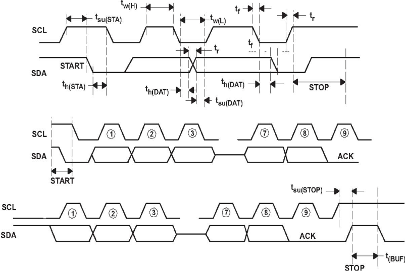 Figure 1. SMBus Communication Timing Waveforms
7.7 Typical Characteristics
Table 1. Table of Graphs
| FIGURE | |
|---|---|
| VCC, ACDET, REGN and ACOK Power Up (bq24707) | Figure 2 |
| Charge Enable by ILIM | Figure 3 |
| Current Soft-Start | Figure 4 |
| Charge Disable by ILIM | Figure 5 |
| Continuous Conduction Mode Switching Waveforms | Figure 6 |
| Cycle-by-Cycle Synchronous to Nonsynchronous | Figure 7 |
| 100% Duty and Refresh Pulse | Figure 8 |
| System Load Transient (Input DPM) | Figure 9 |
| Battery Insertion | Figure 18 |
| Battery-to-Ground Short Protection | Figure 10 |
| Battery-to-Ground Short Transition | Figure 11 |
| Efficiency vs Output Current | Figure 19 |
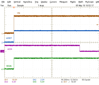
CH1: VCC, 10 V/div; CH2: ACDET, 2 V/div; CH3: ACOK, 5 V/div; CH4: REGN, 5 V/div, 200 ms/div
Figure 2. VCC, ACDET, REGN and ACOK Power Up (bq24707)
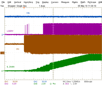
CH1: PHASE, 10 V/div; CH2: Vin, 10 V/div; CH3: LODRV, 5 V/div; CH4: inductor current, 2 A/div, 2 ms/div
Figure 4. Current Soft-Start
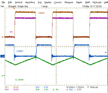
CH1: HIDRV, 10 V/div; CH2: LODRV, 5 V/div; CH3: PHASE,
10 V/div; CH4: inductor current, 2 A/div, 400 ns/div
Figure 6. Continuous Conduction Mode Switching Waveforms
10 V/div; CH4: inductor current, 2 A/div, 400 ns/div
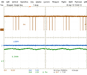
CH1: PHASE, 10 V/div; CH2: LODRV, 5 V/div;
CH4: inductor current, 2 A/div, 4 µs/div
Figure 8. 100% Duty and Refresh Pulse
CH4: inductor current, 2 A/div, 4 µs/div
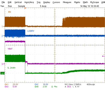
CH1: PHASE, 20 V/div; CH2: LODRV, 10 V/div; CH3: battery voltage, 5 V/div; CH4: inductor current, 2 A/div, 2 ms/div
Figure 10. Battery-to-Ground Short Protection
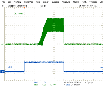
CH2: ILIM, 1 V/div; CH4: inductor current, 1 A/div, 10 ms/div
Figure 3. Charge Enable by ILIM
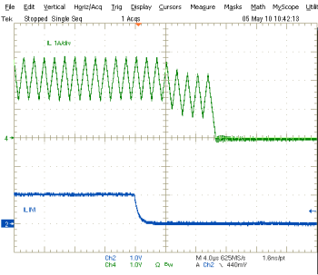
CH2: ILIM, 1 V/div; CH4: inductor current, 1 A/div, 4 µs/div
Figure 5. Charge Disable by ILIM
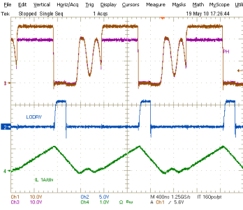
CH1: HIDRV, 10 V/div; CH2: LODRV, 5 V/div; CH3: PHASE,
10 V/div; CH4: inductor current, 1 A/div, 400 ns/div
Figure 7. Cycle-by-Cycle Synchronous to Nonsynchronous
10 V/div; CH4: inductor current, 1 A/div, 400 ns/div
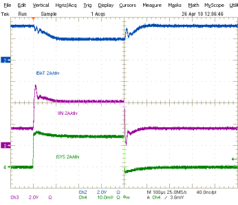
CH2: battery current, 2 A/div; CH3: adapter current, 2 A/div;
CH4: system load current, 2 A/div, 100 µs/div
Figure 9. System Load Transient (Input DPM)
CH4: system load current, 2 A/div, 100 µs/div
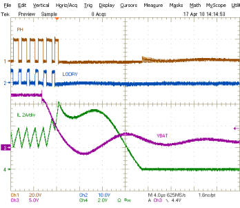
CH1: PHASE, 20 V/div; CH2: LODRV, 10 V/div; CH3: battery voltage, 5 V/div; CH4: inductor current, 2 A/div, 4 µs/div
Figure 11. Battery-to-Ground Short Transition