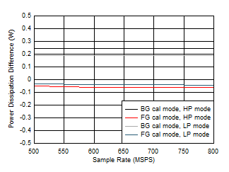
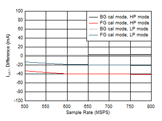
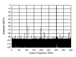
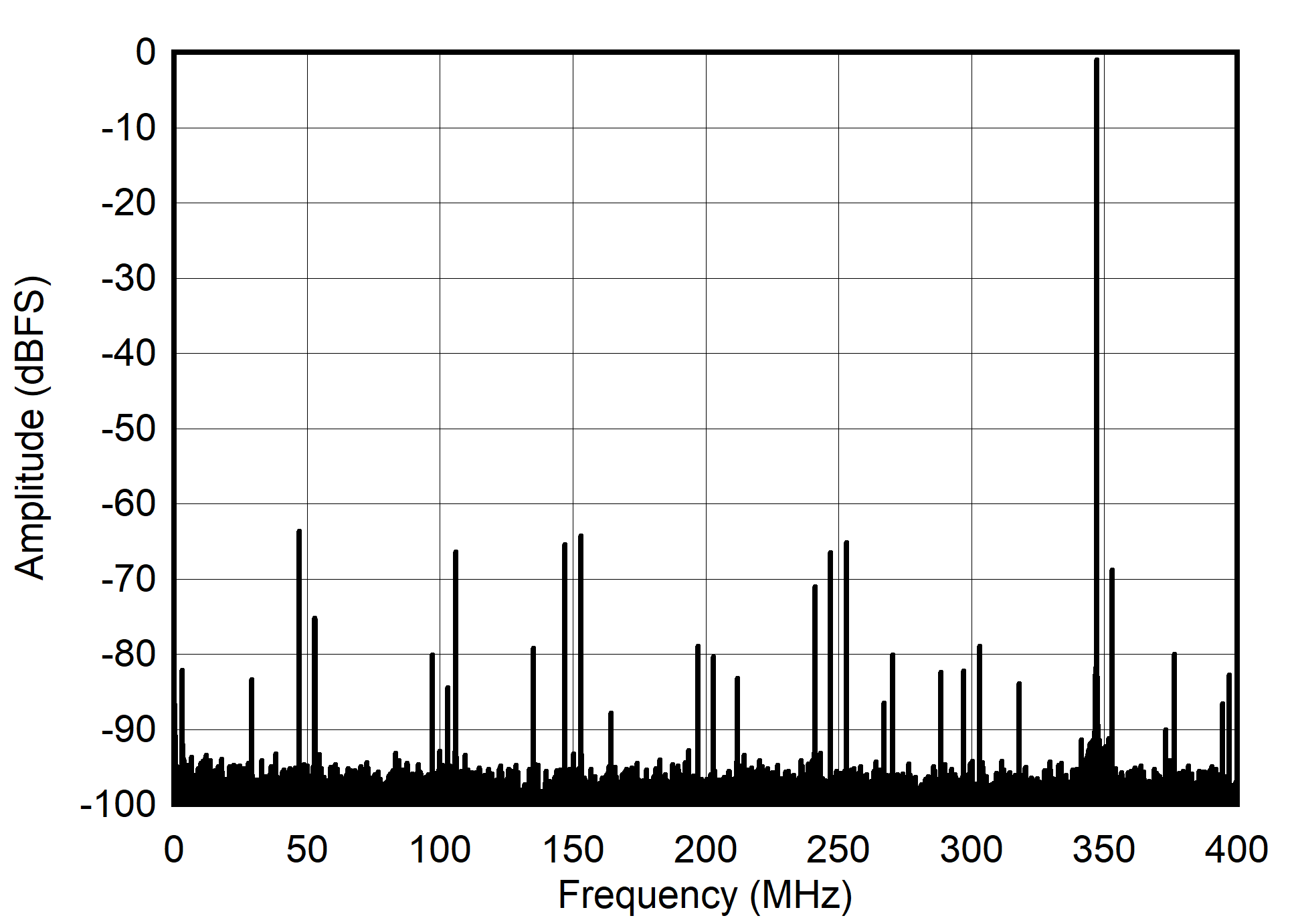
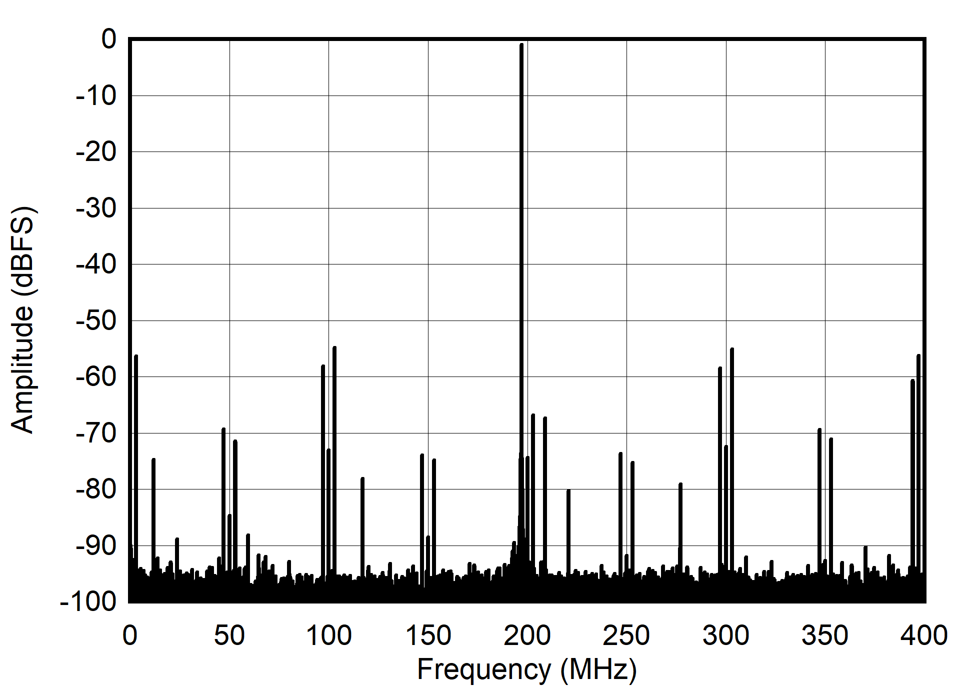
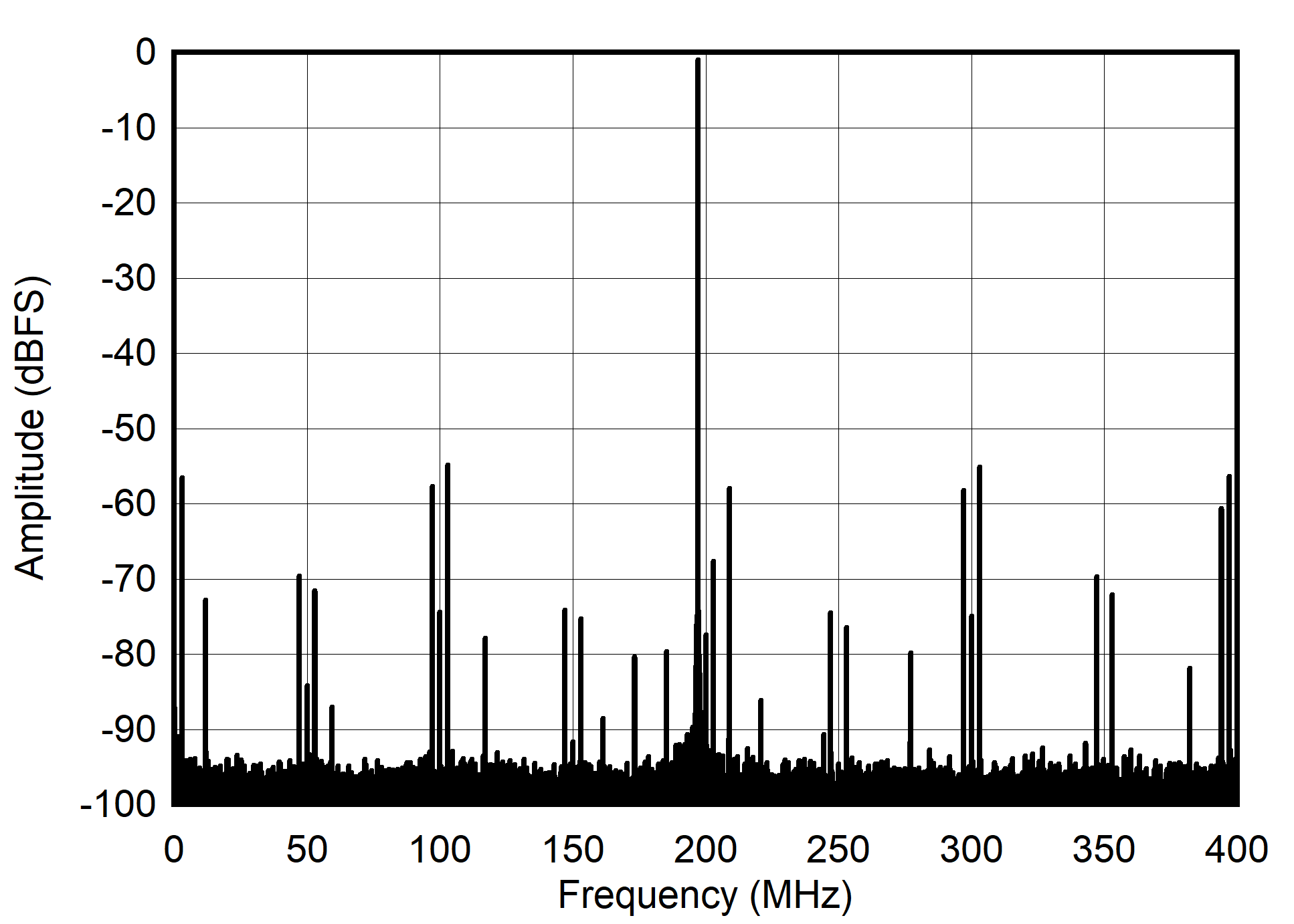
Typical values at 25°C, AIN
= -1 dBFS, FIN = 347 MHz, FS = 800 MSPS, High power mode, FG
calibration, JMODE 0, CPLL off, CPLLREF = 50 MHz and VA11Q and VCLK11
noise suppression on when CPLL on, nominal supply voltages, unless otherwise noted.
SNR results exclude DC, HD2 to HD9; SINAD, ENOB, and SFDR results exclude DC.
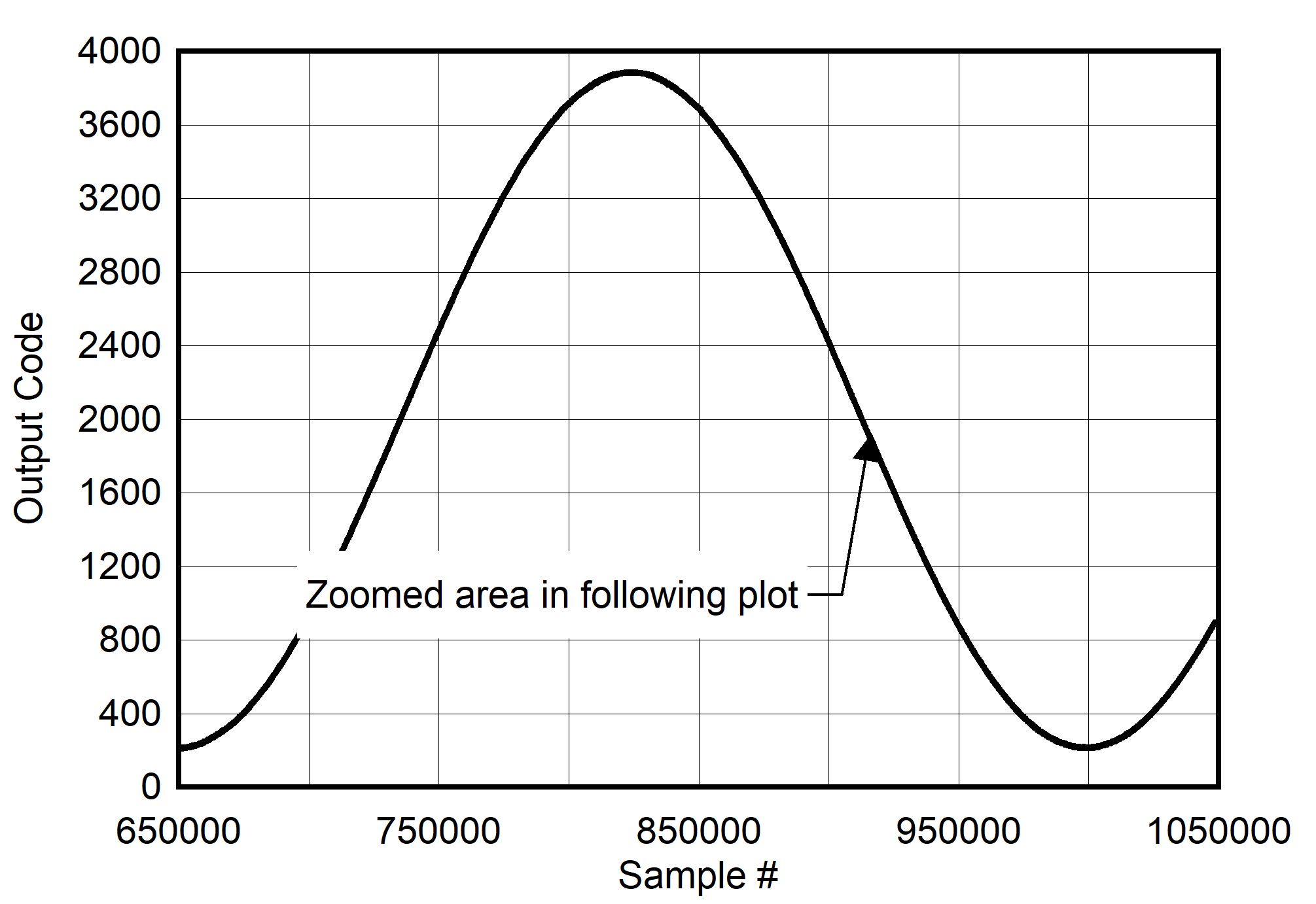
 Figure 5-1 DNL
vs Code
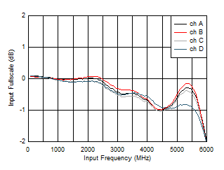
 Figure 5-3 Input
Fullscale vs Input Frequency
 Figure 5-5 Crosstalk vs Input Frequency, Channel B victim
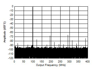
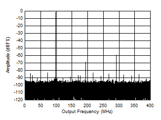
 Figure 5-7 Single Tone FFT at 897 MHz and -1dBFS
 Figure 5-9 Single Tone FFT at 3247 MHz and -1dBFS
 Figure 5-11 Single Tone FFT at 897 MHz and -1dBFS
 Figure 5-13 Single Tone FFT at 3247 MHz and -1dBFS
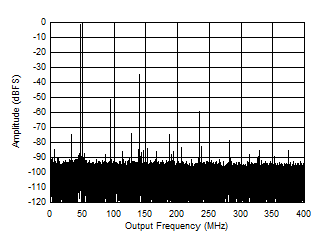
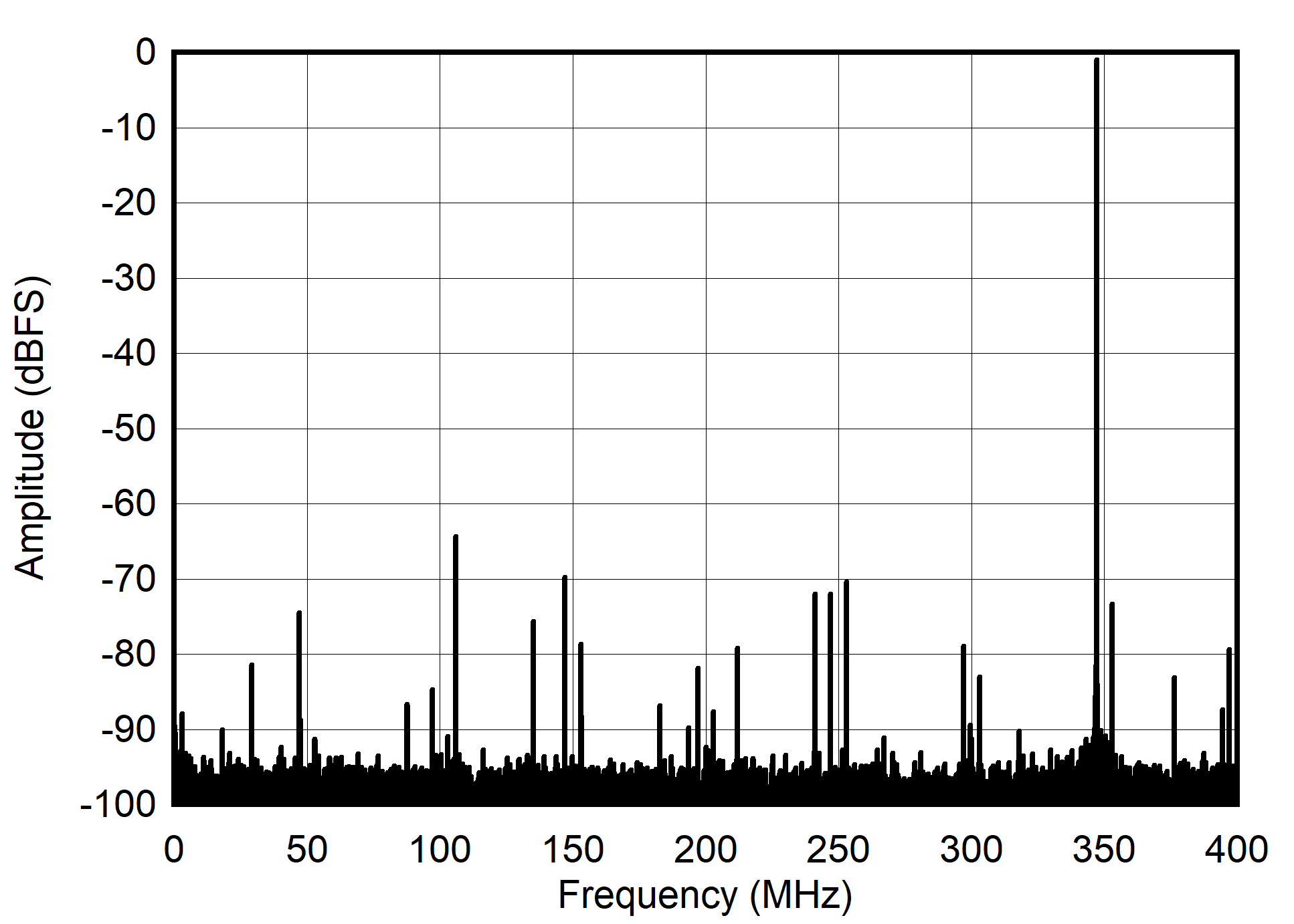
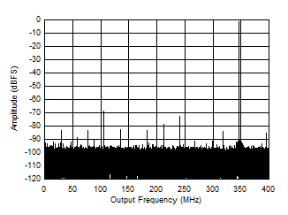
 Figure 5-15 Single Tone FFT at 347 MHz and -1dBFS
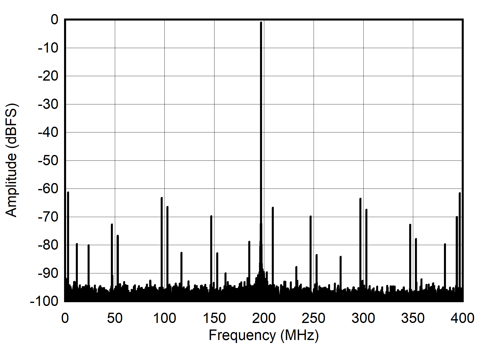
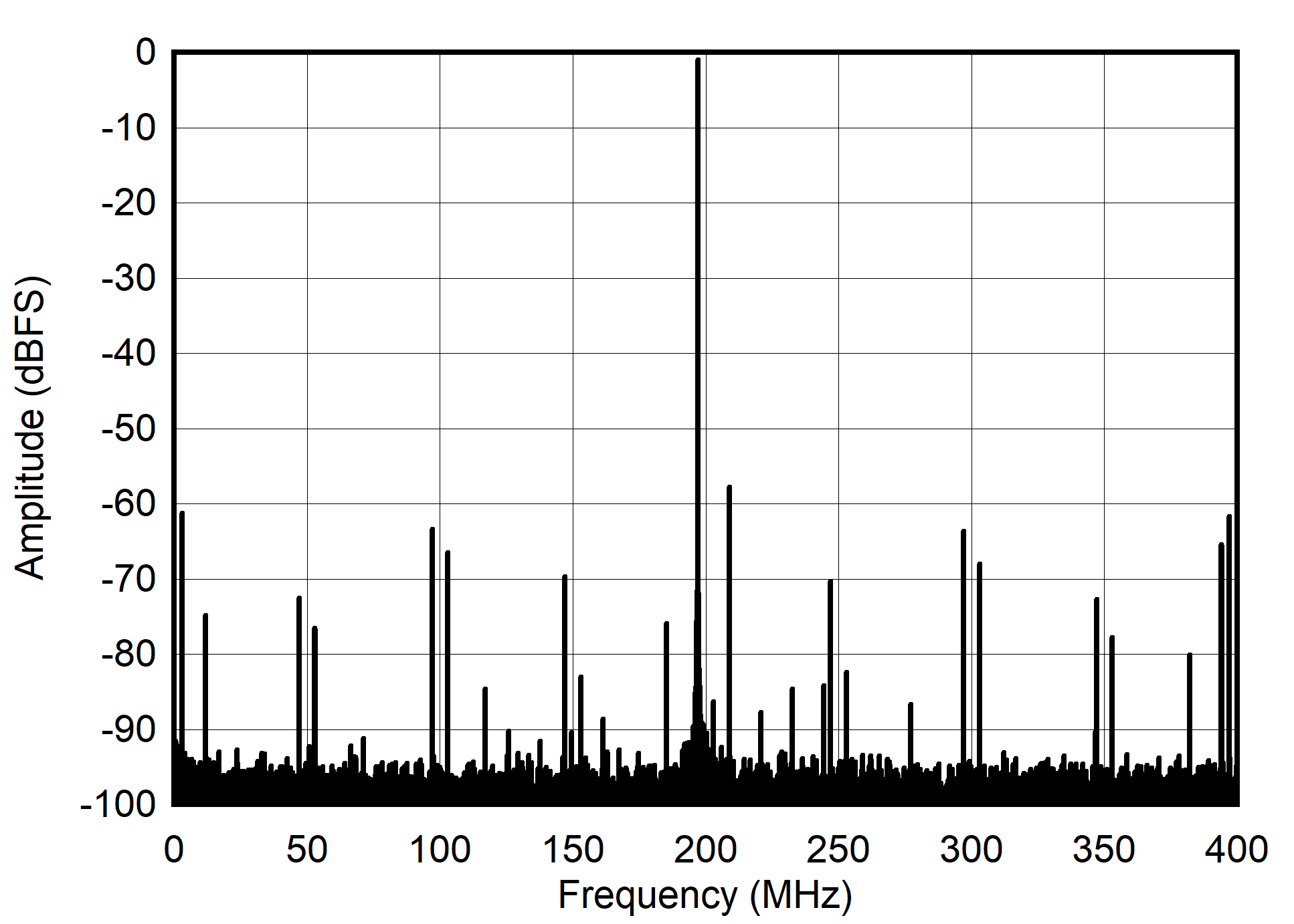
 Figure 5-17 Single Tone FFT at 997 MHz and -1dBFS
| Low
Lower Mode, PLL on, suppression on |

| Low
Lower Mode, PLL on, suppression on |
 Figure 5-23 SFDR
vs Input Frequency
 Figure 5-25 HD3
vs Input Frequency
 Figure 5-27 ENOB
vs Input Frequency
 Figure 5-29 SFDR
vs Sample Rate
 Figure 5-31 ENOB
vs Sample Rate
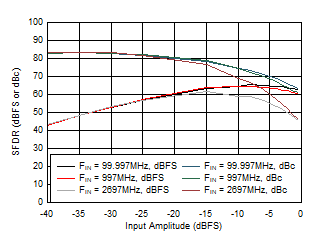
 Figure 5-33 SFDR
vs Input Amplitude
 Figure 5-35 SFDR
vs Input Frequency and Suppression
 Figure 5-37 ENOB
vs Input Frequency and Suppression
| All
supplies moved together |
 Figure 5-41 SFDR
vs Clock Amplitude
 Figure 5-43 SNR
vs Temperature
 Figure 5-45 HD2
vs Temperature
 Figure 5-47 worst
non-HD spur vs Temperature
 Figure 5-49 SFDR
vs Input Frequency in Low Power Mode
 Figure 5-51 HD3
vs Input Frequency in Low Power Mode
 Figure 5-53 ENOB
vs Input Frequency in Low Power Mode
 Figure 5-55 SFDR
vs Sample Rate in Low Power Mode
 Figure 5-57 ENOB
vs Sample Rate in Low Power Mode
 Figure 5-59 SFDR
vs Input Amplitude in Low Power Mode
 Figure 5-61 SFDR
vs Input Frequency
 Figure 5-63 ENOB
vs Input Frequency
| Low
Power Mode, all supplies moved together |
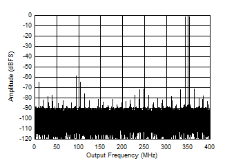
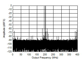
 Figure 5-67 Two
Tone FFT at 1798 MHz
 Figure 5-69 Two
Tone FFT at 347 MHz in Low Power Mode
 Figure 5-71 Two
Tone FFT at 3498 MHz in Low Power Mode
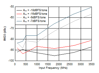
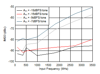
 Figure 5-73 IMD3
vs Input Frequency in Low Power Mode
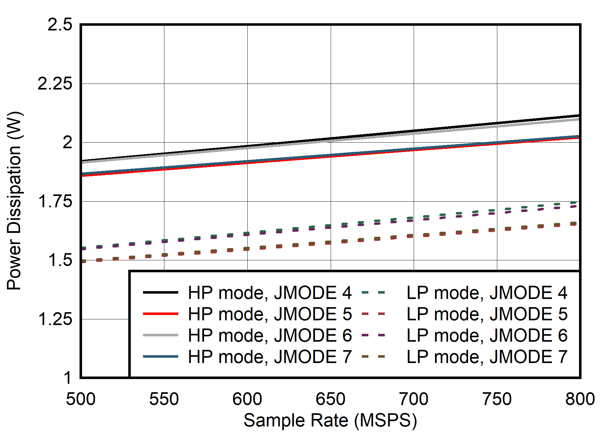
 Figure 5-75 Quad
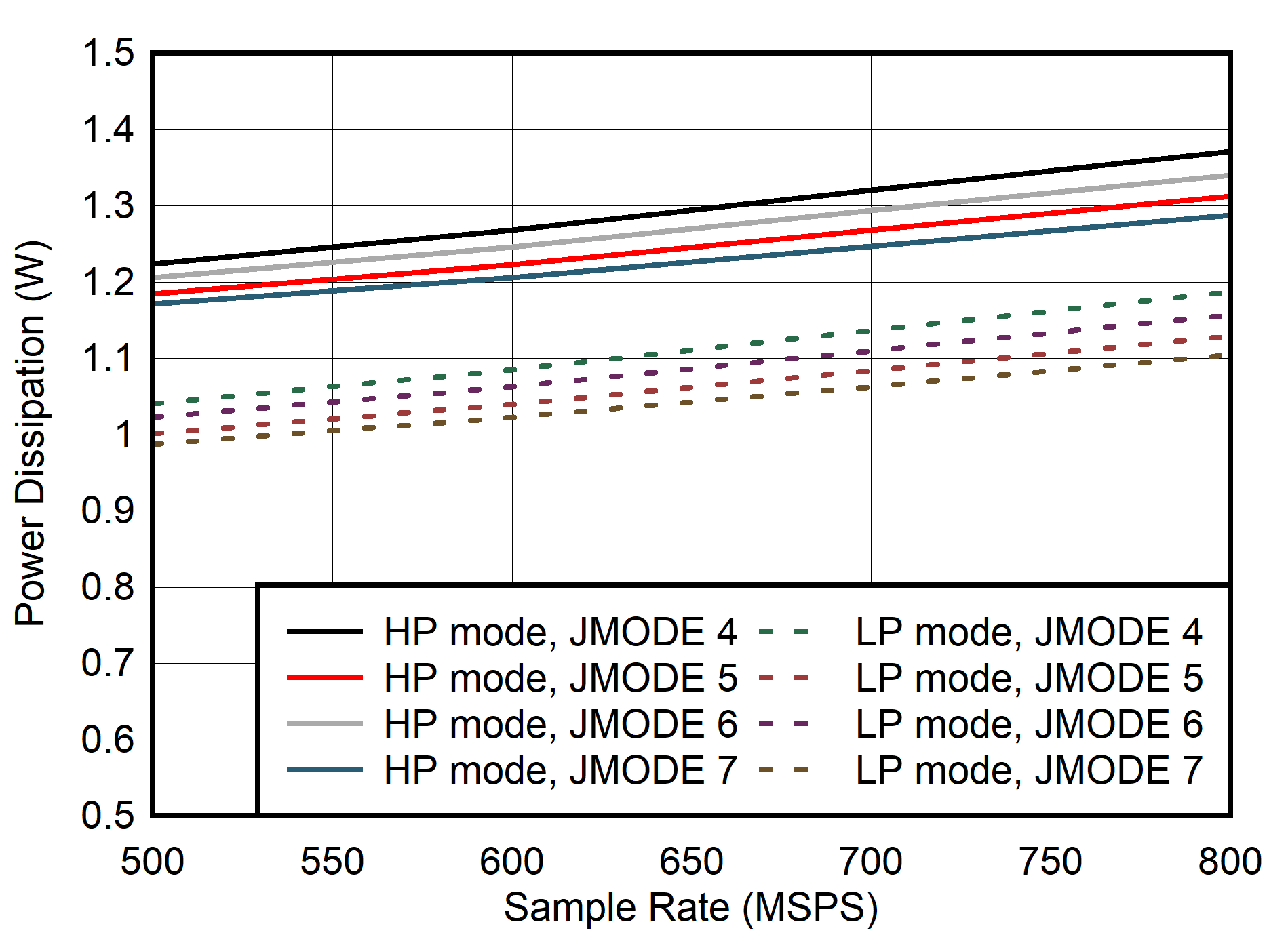
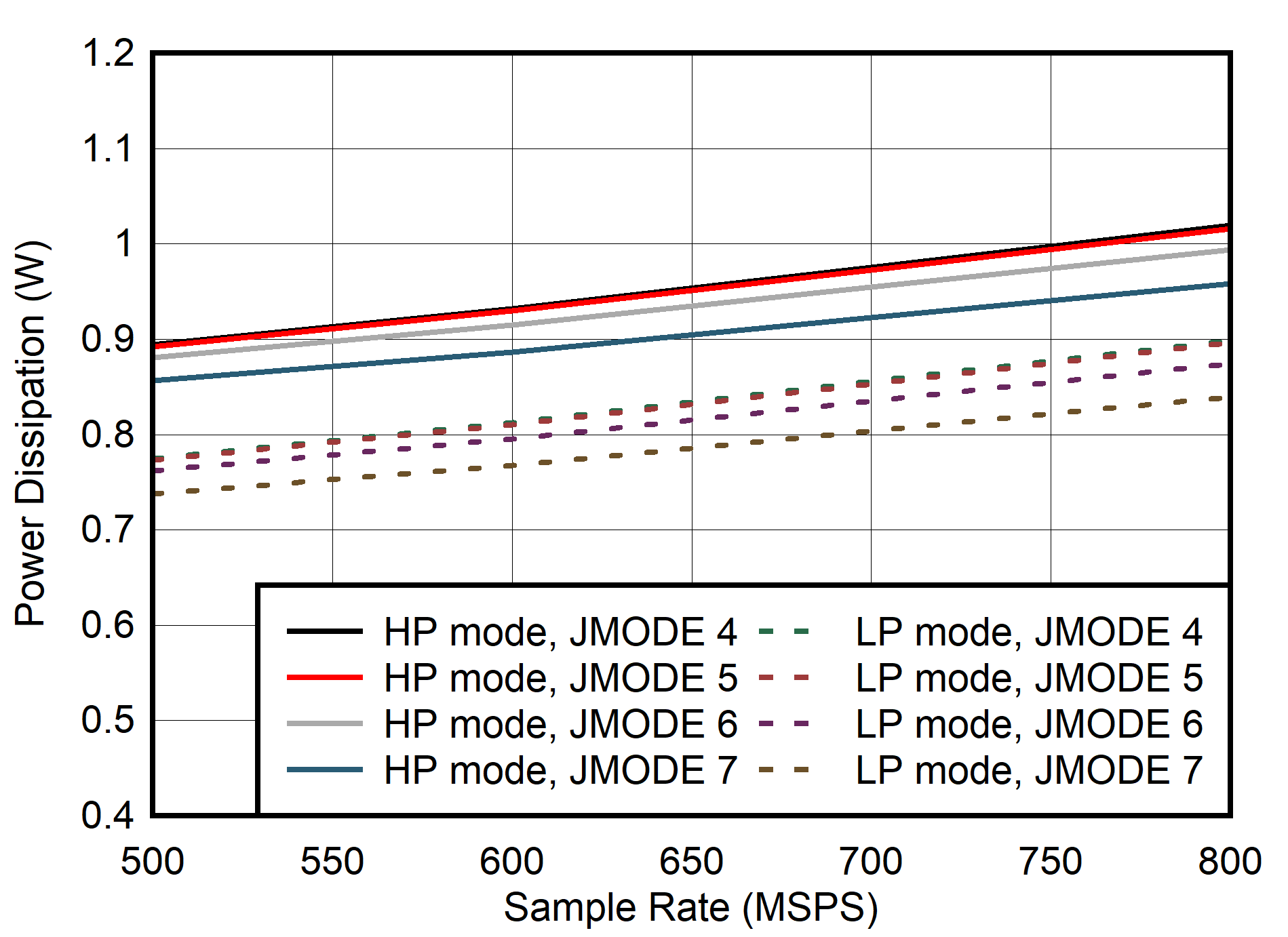
Channel, Power Dissipation vs FS for JMODES 4 - 7
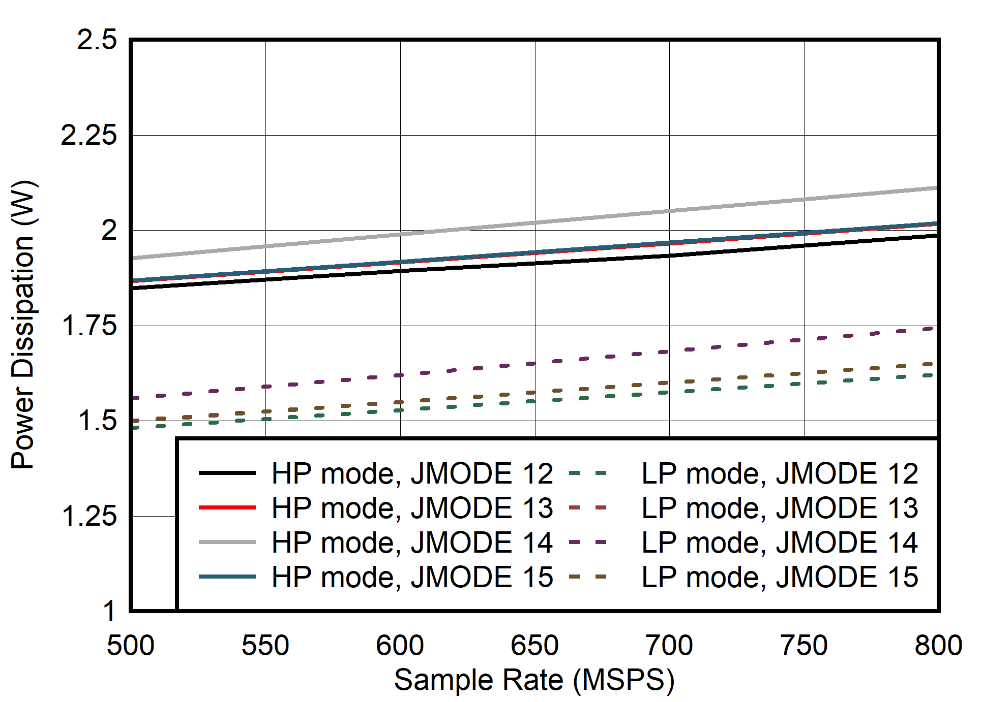
 Figure 5-77 Quad
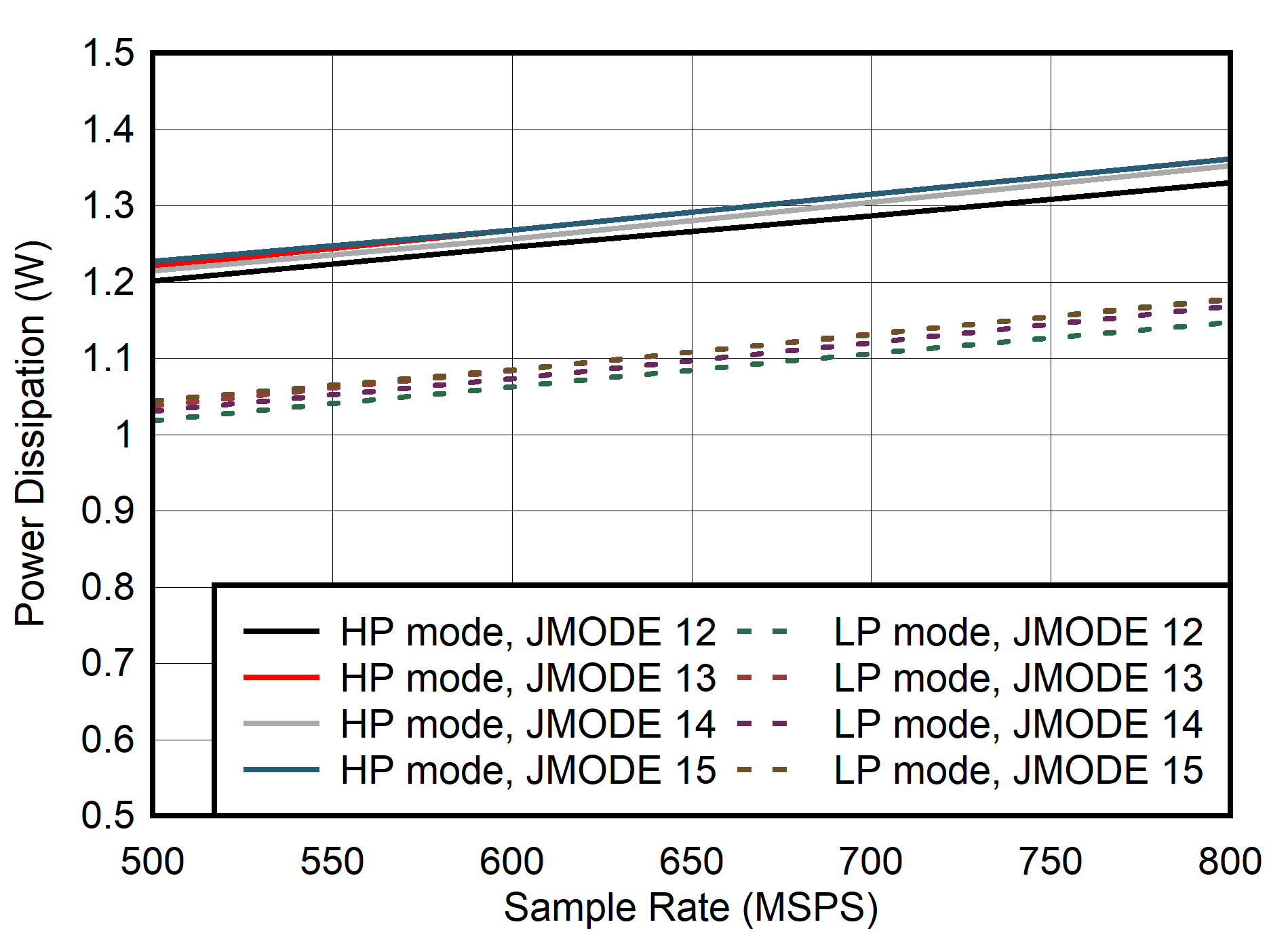
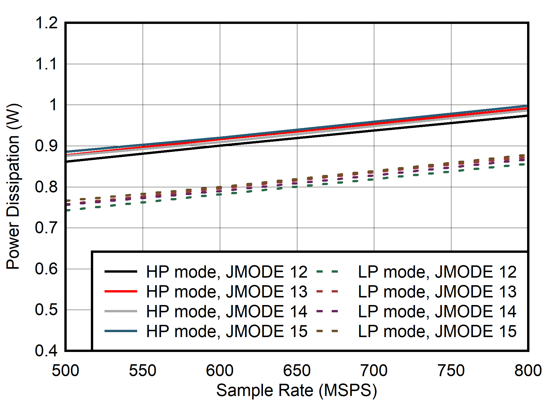
Channel, Power Dissipation vs FS for JMODES 12 - 15
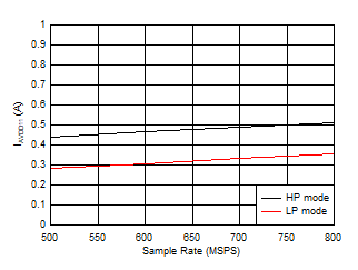
 Figure 5-79 Quad
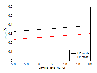
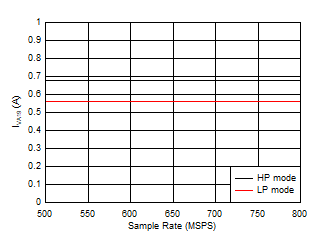
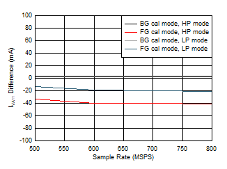
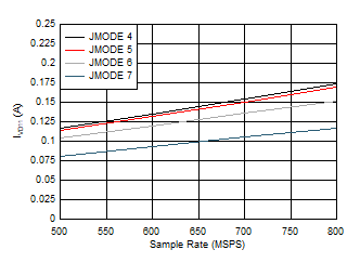
Channel, IVA11 vs FS
| Independent of Power Mode |

| Independent of Power Mode |
 Figure 5-85 Quad
Channel, IVA19 vs FS over Modes
 Figure 5-87 Quad
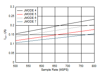
Channel, IVD11 vs FS over Modes
 Figure 5-89 Dual
Channel, Power Dissipation vs FS for JMODES 4 - 7
 Figure 5-91 Dual
Channel, Power Dissipation vs FS for JMODES 12 - 15
 Figure 5-93 Dual
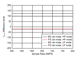
Channel, IVA11 vs FS
 Figure 5-95 Dual
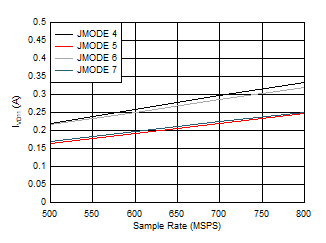
Channel, IVD11 vs FS for JMODES 4 - 7
 Figure 5-97 Dual
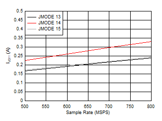
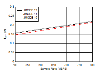
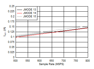
Channel, IVD11 vs FS for JMODES 13 - 15
 Figure 5-99 Dual
Channel, IVA19 vs FS over Modes
 Figure 5-101 Dual
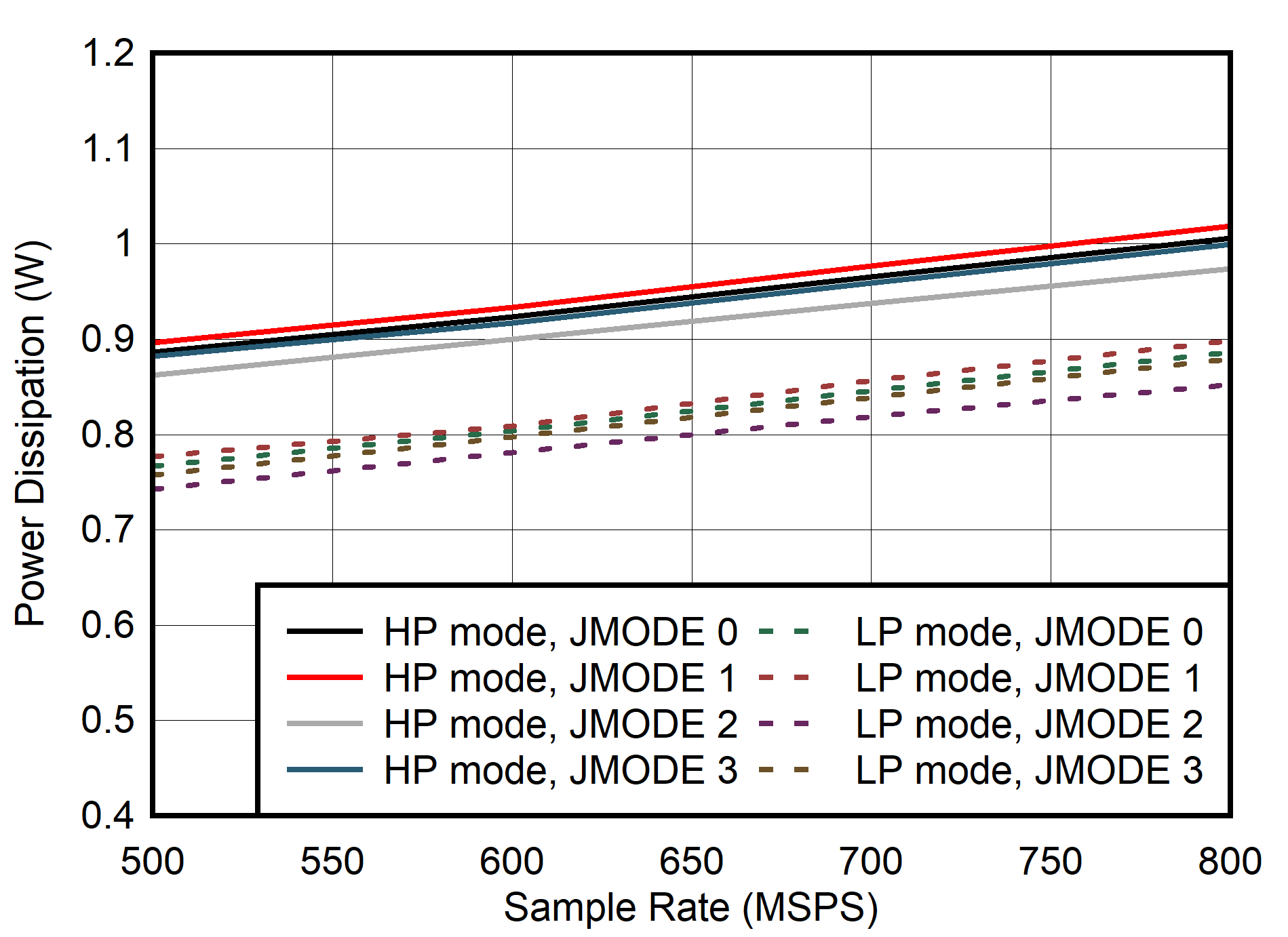
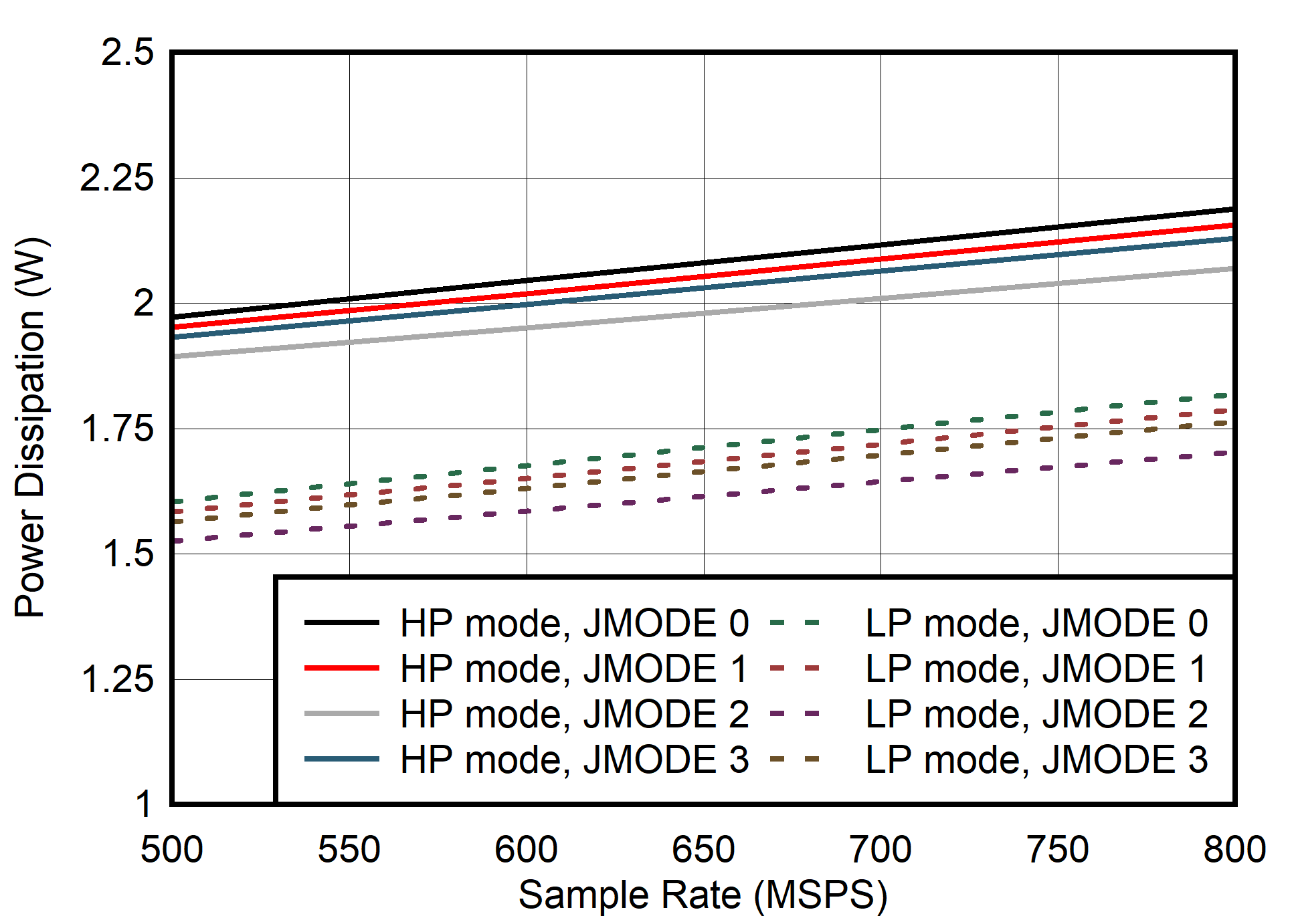
Channel, Power Dissipation vs FS for JMODES 0 - 3
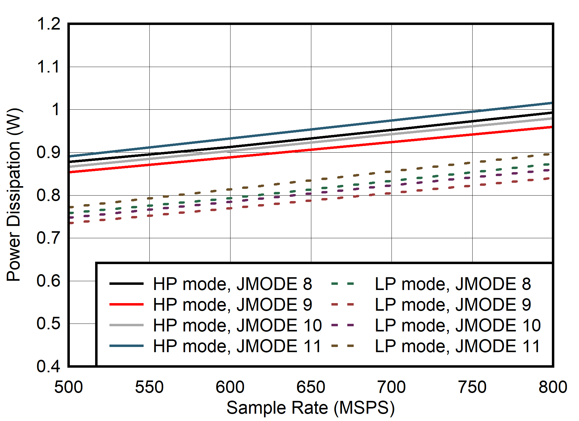
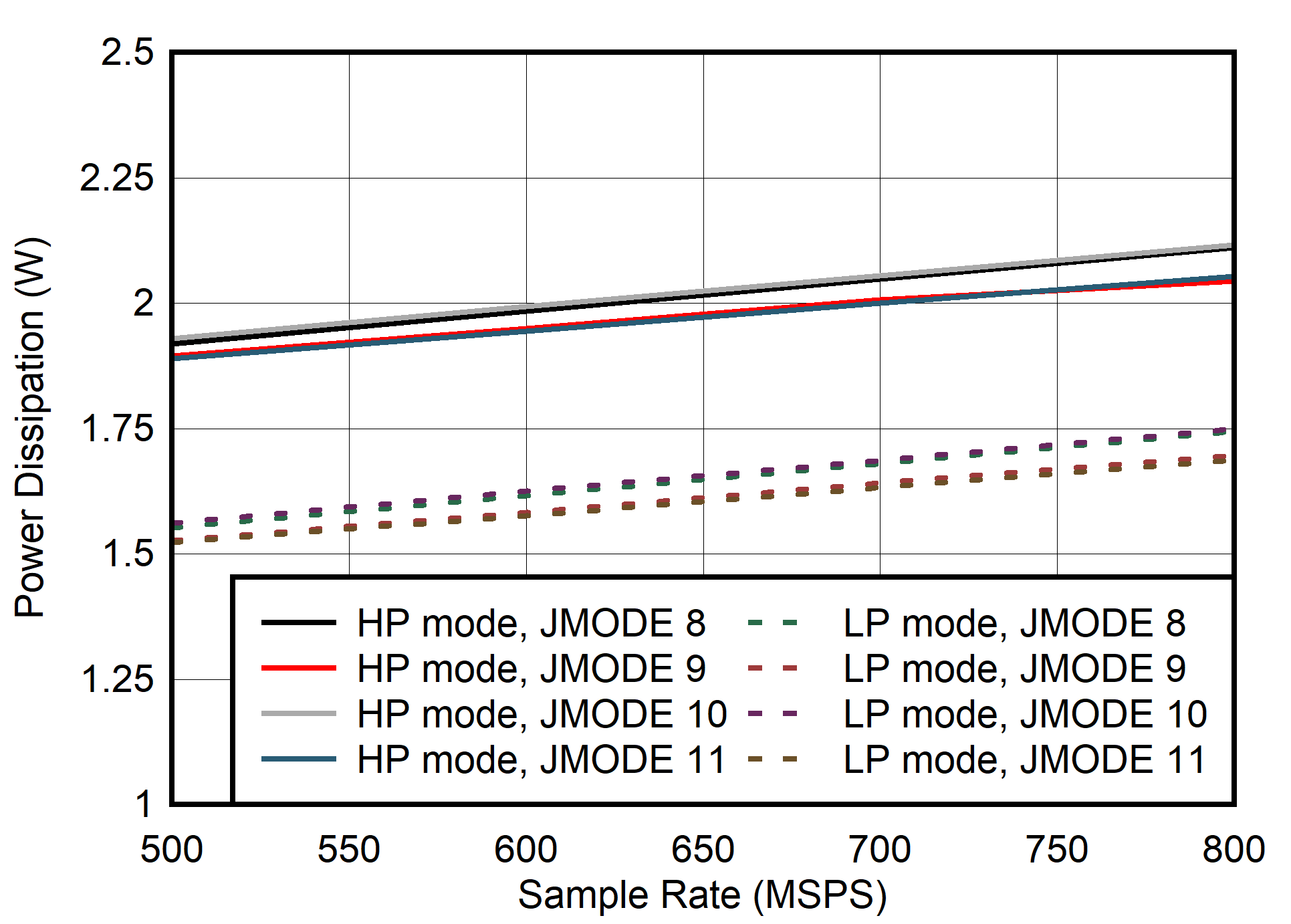
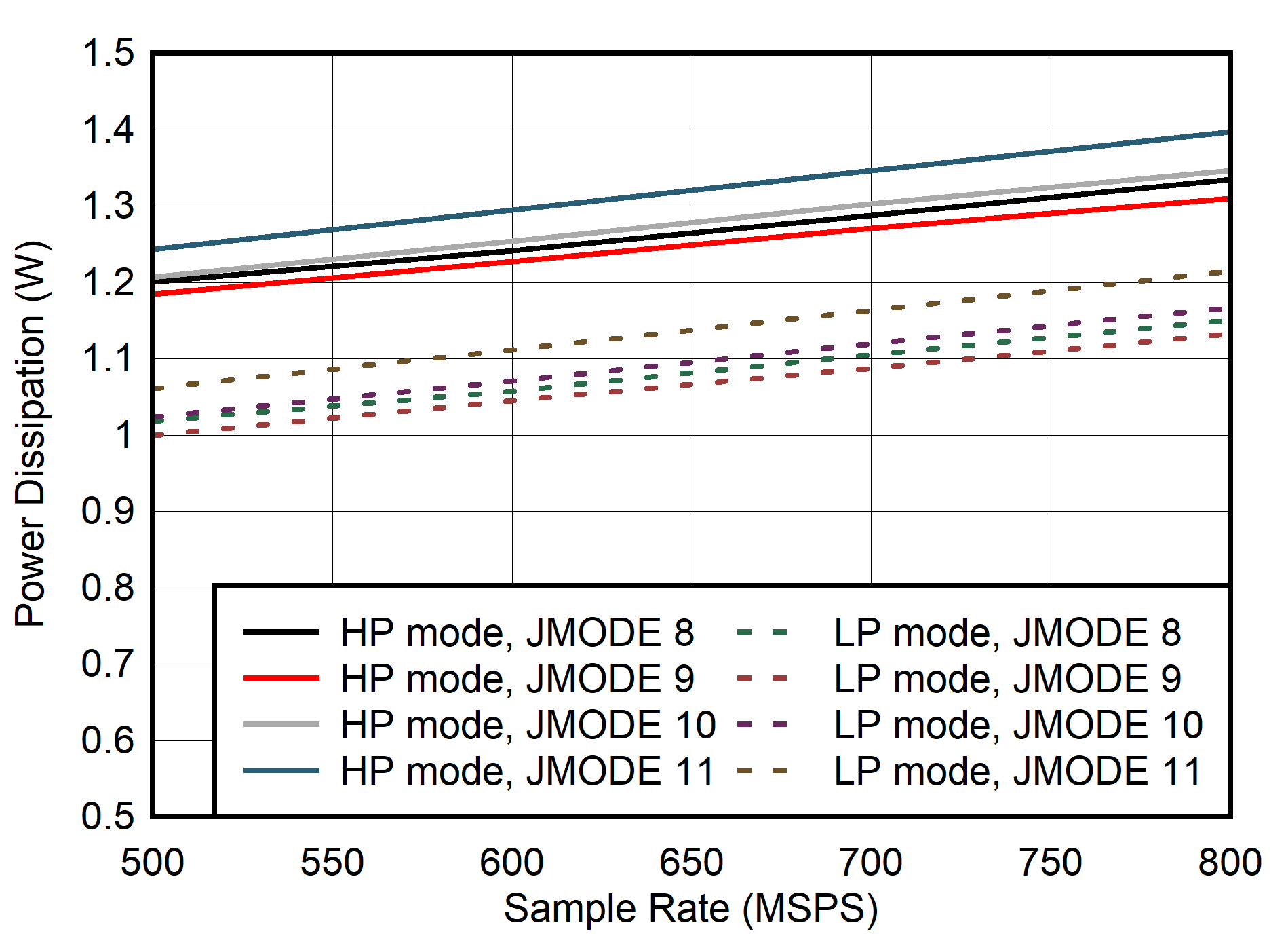
 Figure 5-103 Single Channel, Power Dissipation vs FS for JMODES 8 -
11
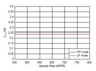
 Figure 5-105 Single Channel, IVA19 vs FS
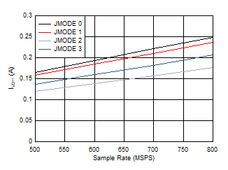
 Figure 5-107 Single Channel, IVD11 vs FS for JMODES 0 - 3
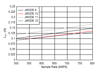
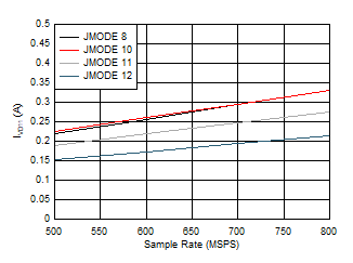
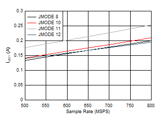
 Figure 5-109 Single Channel, IVD11 vs FS for JMODES 8 - 12
 Figure 5-111 Single Channel, Power Dissipation vs FS over Modes
 Figure 5-113 Single Channel, IVA11 vs FS over Modes
| BG
Calibration, midscale input voltage, ADC_SRC_DLY=31,
MUX_DLY=30 |

| BG
Calibration, midscale input voltage, ADC_SRC_DLY=31,
MUX_DLY=30 |
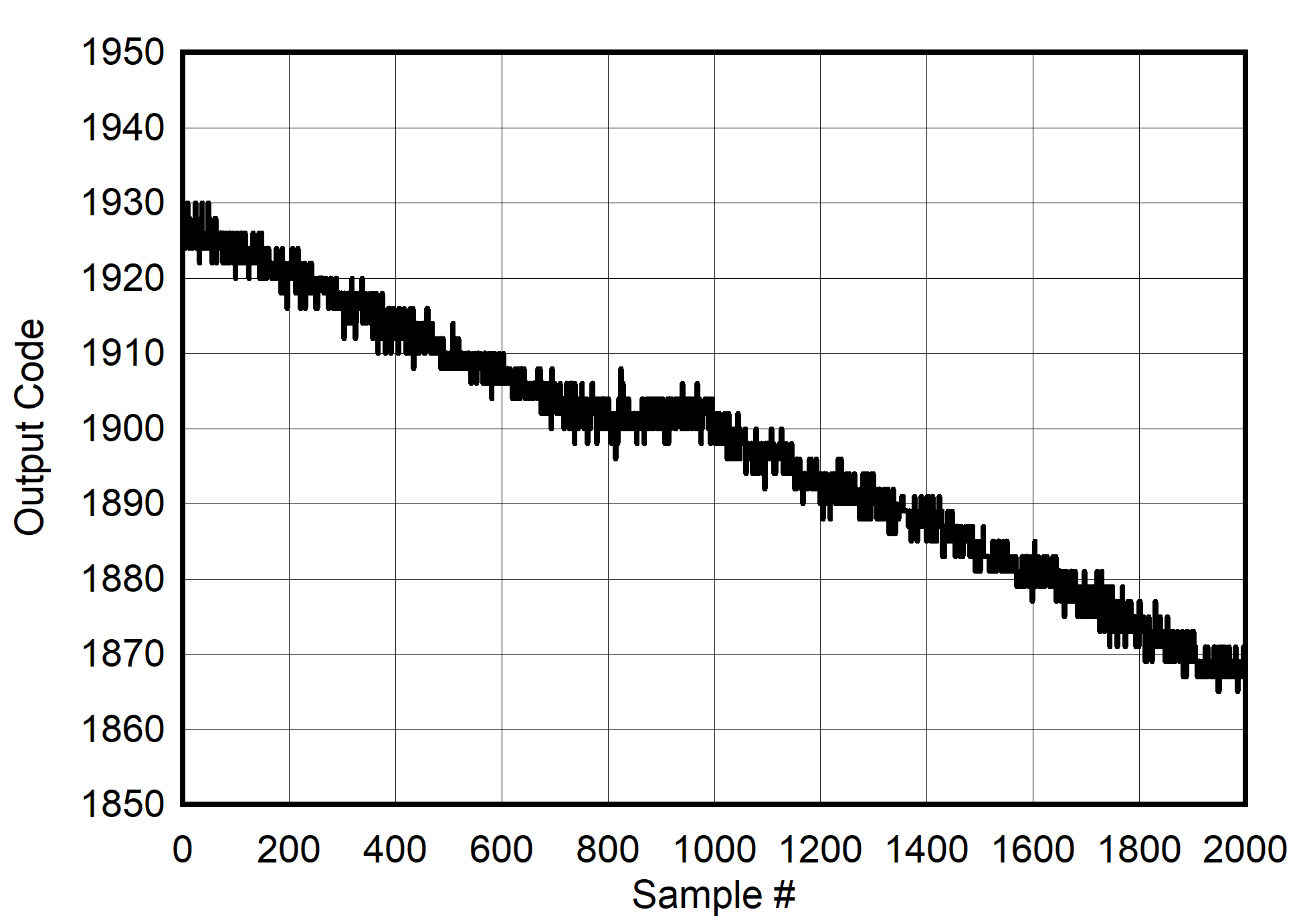
 Figure 5-2 INL
vs Code
 Figure 5-4 Crosstalk vs Input Frequency, Channel A victim
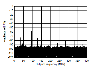
 Figure 5-6 Single Tone FFT at 347 MHz and -1dBFS
 Figure 5-8 Single Tone FFT at 2097 MHz and -1dBFS
 Figure 5-10 Single Tone FFT at 347 MHz and -1dBFS
 Figure 5-12 Single Tone FFT at 2097 MHz and -1dBFS
 Figure 5-14 Single Tone FFT at 347 MHz and -1dBFS
 Figure 5-16 Single Tone FFT at 997 MHz and -1dBFS
| Low
Lower Mode, PLL on, suppression off |

| Low
Lower Mode, PLL on, suppression off |
 Figure 5-22 SNR
vs Input Frequency
 Figure 5-24 HD2
vs Input Frequency
 Figure 5-26 SINAD
vs Input Frequency
 Figure 5-28 SNR
vs Sample Rate
 Figure 5-30 SINAD
vs Sample Rate
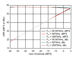
 Figure 5-32 SNR
vs Input Amplitude
 Figure 5-34 SNR
vs Input Frequency and Suppression
 Figure 5-36 SINAD
vs Input Frequency and Suppression
| All
supplies moved together |
 Figure 5-40 SNR
vs Clock Amplitude
 Figure 5-42 SNR,
SFDR and SINAD vs Reference Frequency with PLL on
 Figure 5-44 SFDR
vs Temperature
 Figure 5-46 HD3
vs Temperature
 Figure 5-48 SNR
vs Input Frequency in Low Power Mode
 Figure 5-50 HD2
vs Input Frequency in Low Power Mode
 Figure 5-52 SINAD
vs Input Frequency in Low Power Mode
 Figure 5-54 SNR
vs Sample Rate in Low Power Mode
 Figure 5-56 SINAD
vs Sample Rate in Low Power Mode
 Figure 5-58 SNR
vs Input Amplitude in Low Power Mode
 Figure 5-60 SNR
vs Input Frequency
 Figure 5-62 SINAD
vs Input Frequency
| Low
Power Mode, all supplies moved together |
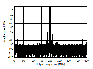
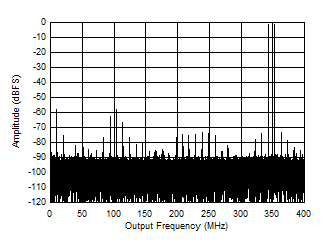
 Figure 5-66 Two
Tone FFT at 347 MHz
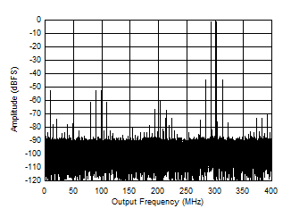
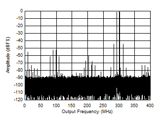
 Figure 5-68 Two
Tone FFT at 3498 MHz
 Figure 5-70 Two
Tone FFT at 1798 MHz in Low Power Mode
 Figure 5-72 IMD3
vs Input Frequency
 Figure 5-74 Quad
Channel, Power Dissipation vs FS for JMODES 0 - 3
 Figure 5-76 Quad
Channel, Power Dissipation vs FS for JMODES 8 - 11
 Figure 5-78 Quad
Channel, IVA19 vs FS
| Independent of Power Mode |

| Independent of Power Mode |
 Figure 5-84 Quad
Channel, Power Dissipation vs FS over Modes
 Figure 5-86 Quad
Channel, IVA11 vs FS over Modes
 Figure 5-88 Dual
Channel, Power Dissipation vs FS for JMODES 0 - 3
 Figure 5-90 Dual
Channel, Power Dissipation vs FS for JMODES 8 - 11
 Figure 5-92 Dual
Channel, IVA19 vs FS
 Figure 5-94 Dual
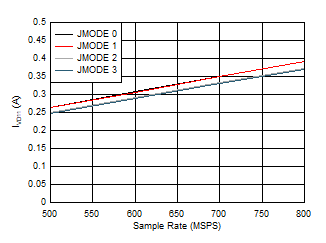
Channel, IVD11 vs FS for JMODES 0 - 3
 Figure 5-96 Dual
Channel, IVD11 vs FS for JMODES 8 - 12
 Figure 5-98 Dual
Channel, Power Dissipation vs FS over Modes
 Figure 5-100 Dual
Channel, IVA11 vs FS over Modes
 Figure 5-102 Single Channel, Power Dissipation vs FS for JMODES 4 - 7
 Figure 5-104 Single Channel, Power Dissipation vs FS for JMODES 12 -
15
 Figure 5-106 Single Channel, IVA11 vs FS
 Figure 5-108 Single Channel, IVD11 vs FS for JMODES 4 - 7
 Figure 5-110 Single Channel, IVD11 vs FS for JMODES 13 -
15
 Figure 5-112 Single Channel, IVA19 vs FS over Modes
 Figure 5-114 Single Channel, IVD11 vs FS over Modes
| BG
Calibration, midscale input voltage, ADC_SRC_DLY=31,
MUX_DLY=30 |

| BG
Calibration, midscale input voltage, ADC_SRC_DLY=31,
MUX_DLY=30 |

