TIDT236 March 2022 TPS7H1101A-SP
Description
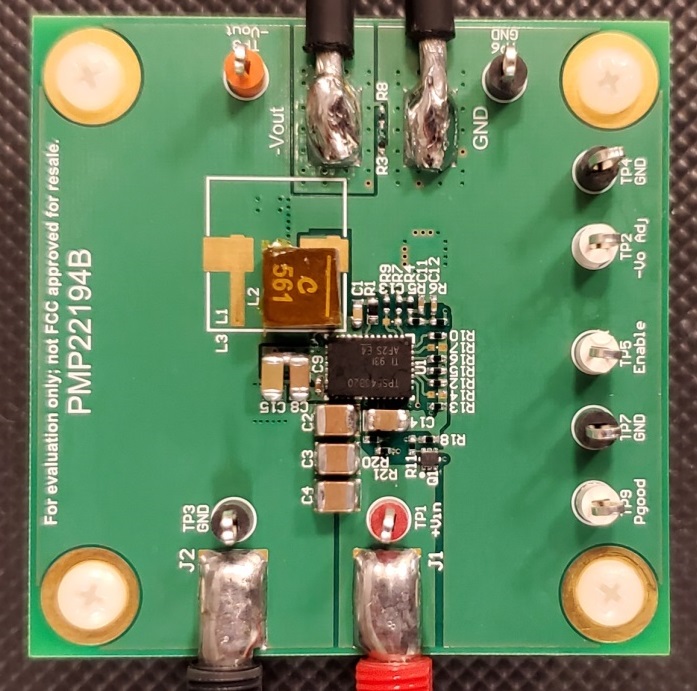
This reference design utilizes a synchronous buck regulator with internal top and bottom FETs, which is configured as a synchronous inverting buck-boost converter to provide an adjustable output of between –0.2 V and –0.6 V capable of delivering a maximum of 15 A of current to the load. The output voltage is adjusted by either providing a PWM signal or analog voltage signal to the –Vout Adj connector, referenced to GND. See the Board Schematic for details regarding voltages.
 Top Side of PCB
 Bottom Side of PCB
 Board Schematic